Basic research on CVD single crystal diamond processing by UV nanosecond laser
-
摘要: 化学气相沉积(chemical vapor deposition,CVD)单晶金刚石因具备优异的材料特性,被广泛应用于散热等领域;但由于CVD单晶金刚石的高硬度及脆性,目前多采用激光进行CVD单晶金刚石微槽结构的加工。为探究激光参数对CVD单晶金刚石微槽结构的影响,通过构建紫外纳秒激光平顶模式的线刻蚀能量模型并结合线刻蚀试验,分析激光功率及扫描速度对刻蚀CVD单晶金刚石槽宽度及深度的影响规律。结果表明:在线刻蚀试验中,激光功率由1.2 W增大至10.8 W时,线刻蚀槽的宽度基本不变,而深度由35.7 μm增大至57.2 μm;扫描速度由3 mm/s增大至29 mm/s时,线刻蚀槽的宽度由39.5 μm缩减至26.3 μm,深度由77.6 μm缩减至18.0 μm。结合线刻蚀能量模型以及线刻蚀试验,激光功率的增大会导致线刻蚀槽的宽度和深度增大,但对深度的影响要大于对宽度的影响;扫描速度的增大会导致槽的宽度和深度减小,同时导致槽锥角增大,底部出现平坦面。此外,EDS分析显示激光刻蚀后的产物中C元素含量减少,而O、N元素含量增加,说明在刻蚀过程中可能发生了金刚石向石墨的相变以及石墨的氧化反应,且在线刻蚀过程中可能出现了反应产物的溅射现象。Abstract:
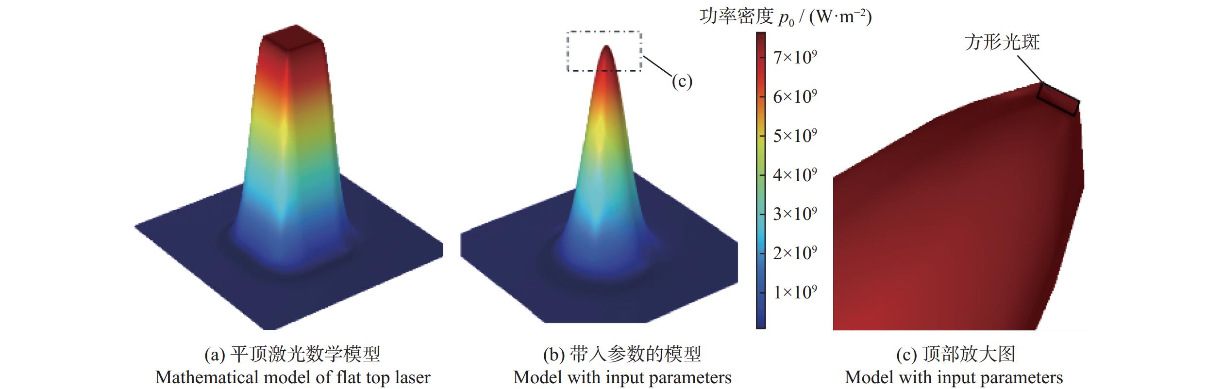
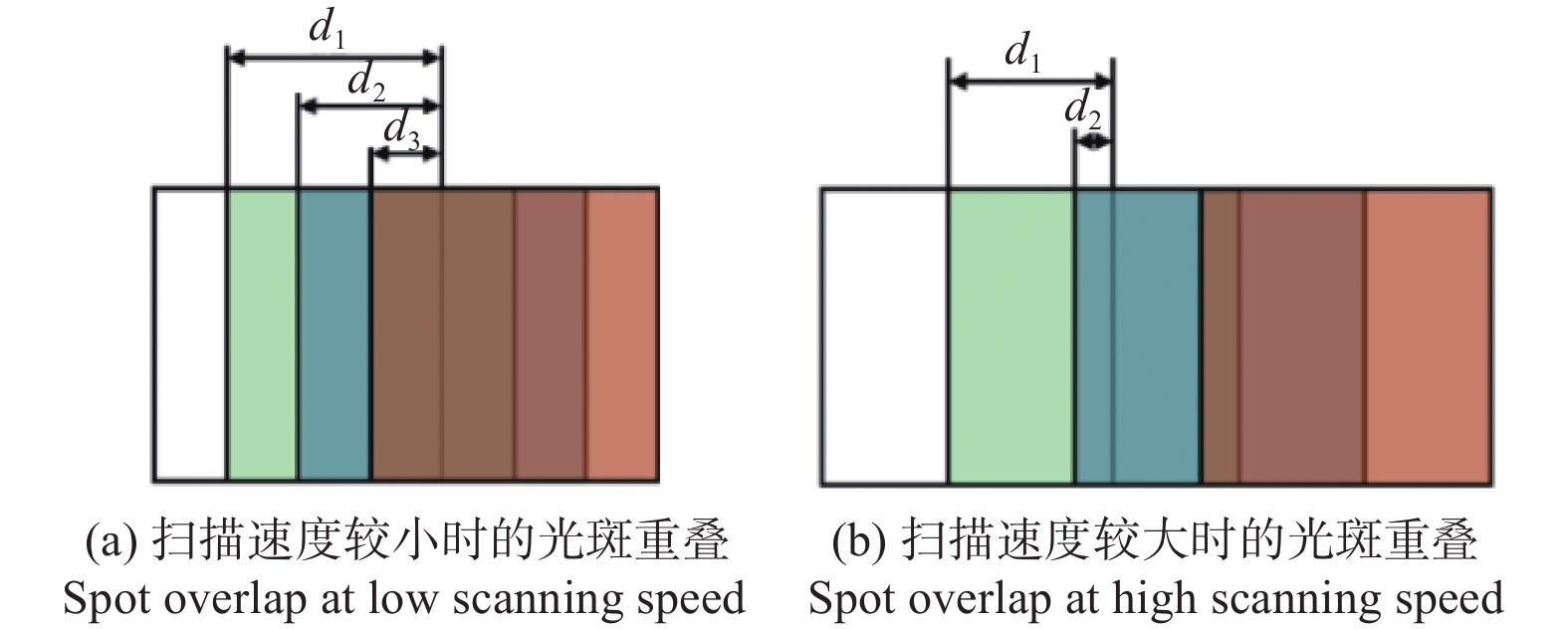
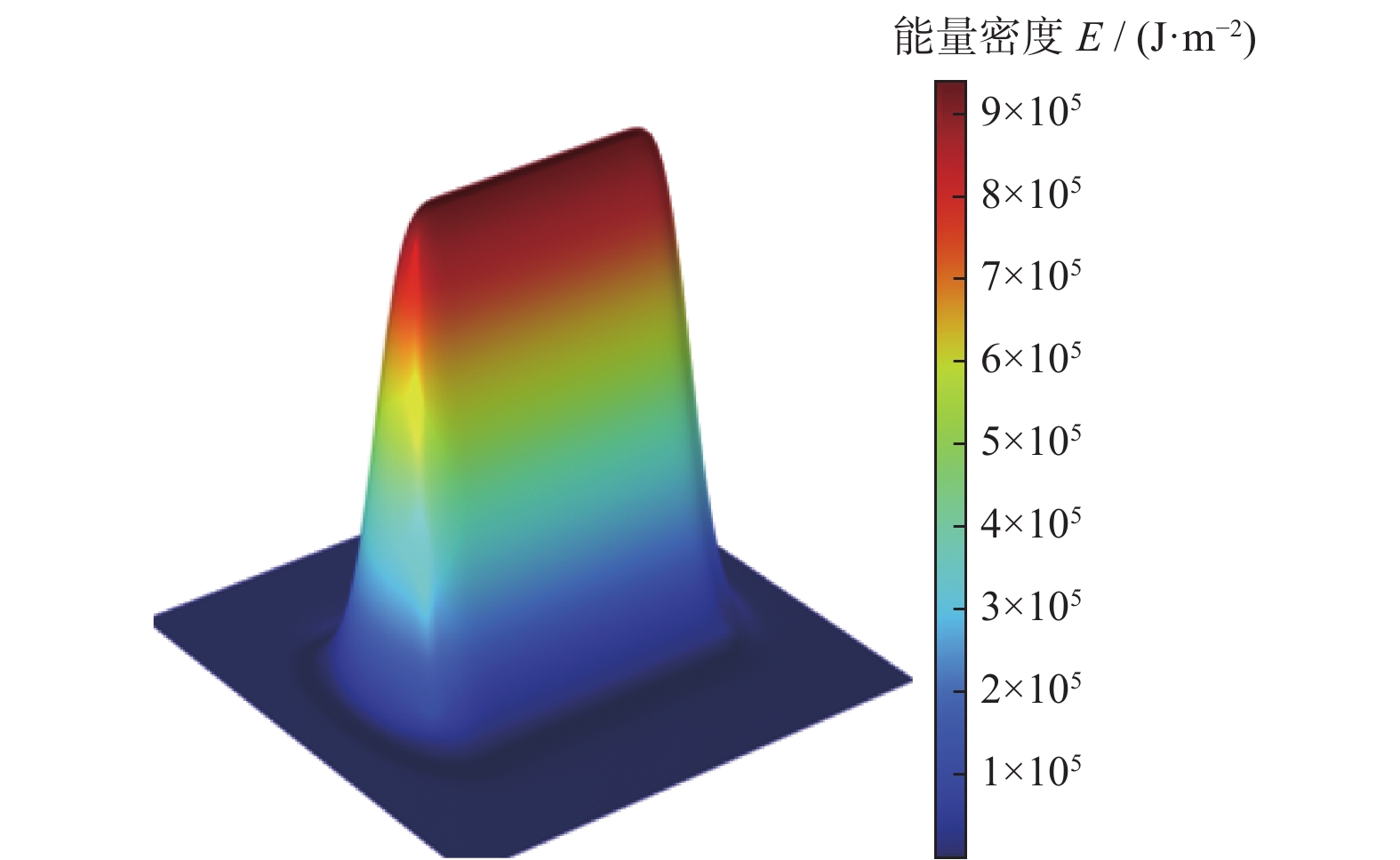
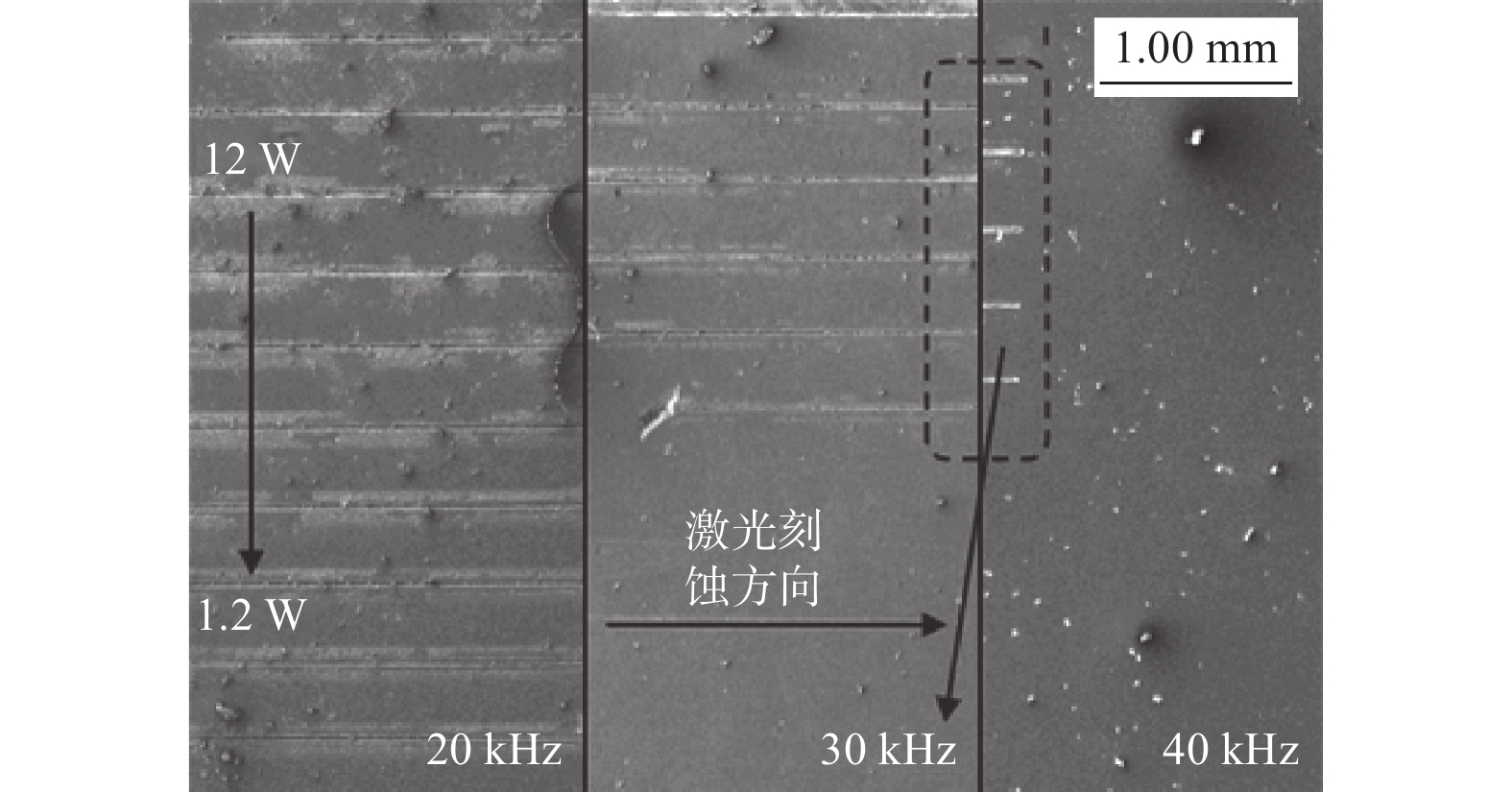
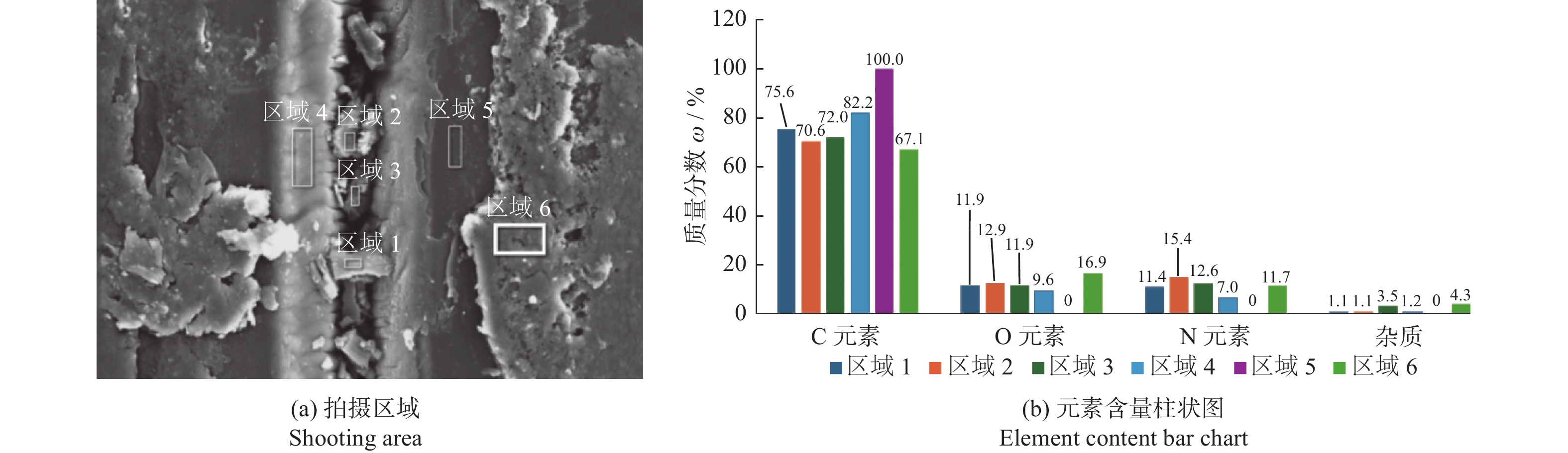
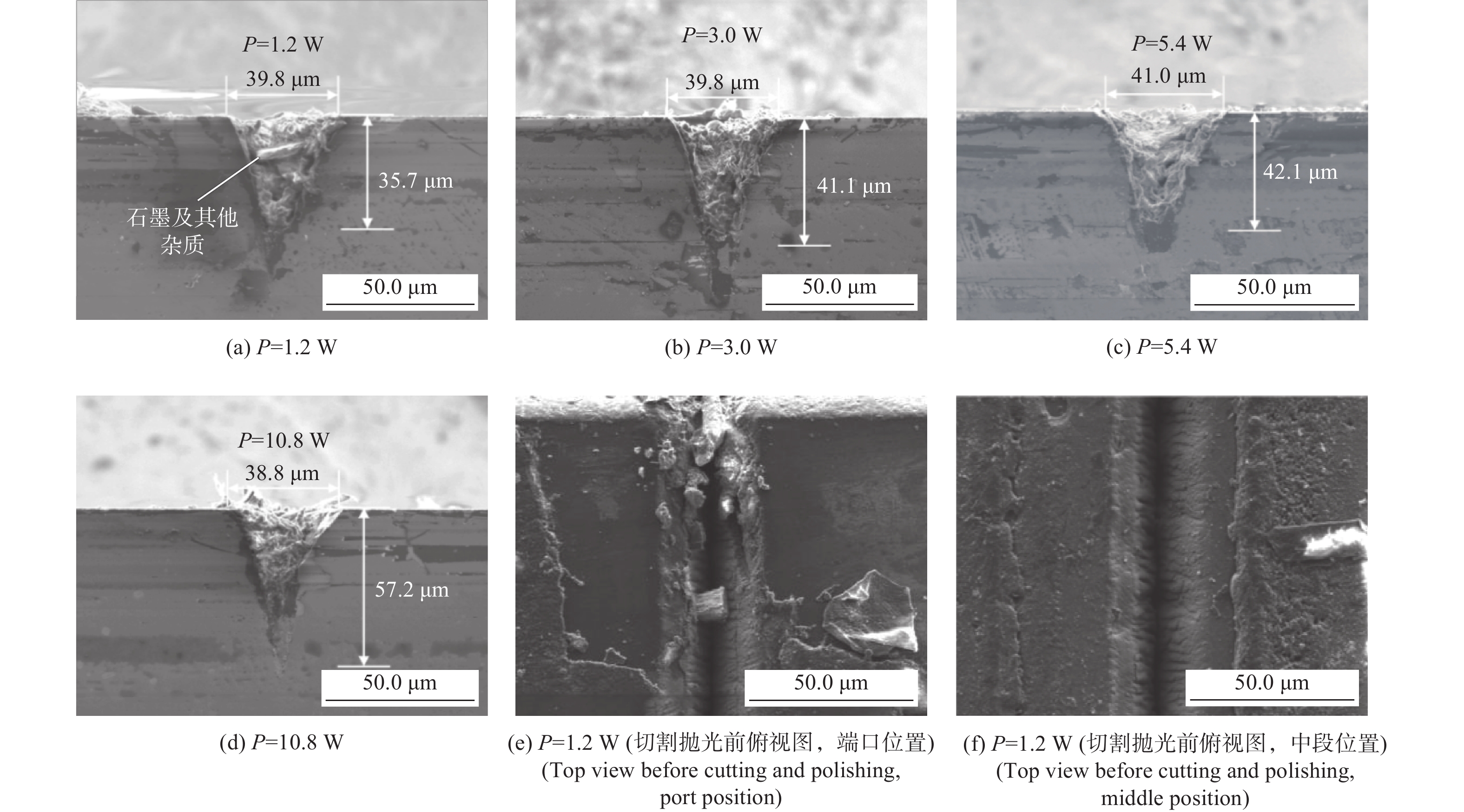
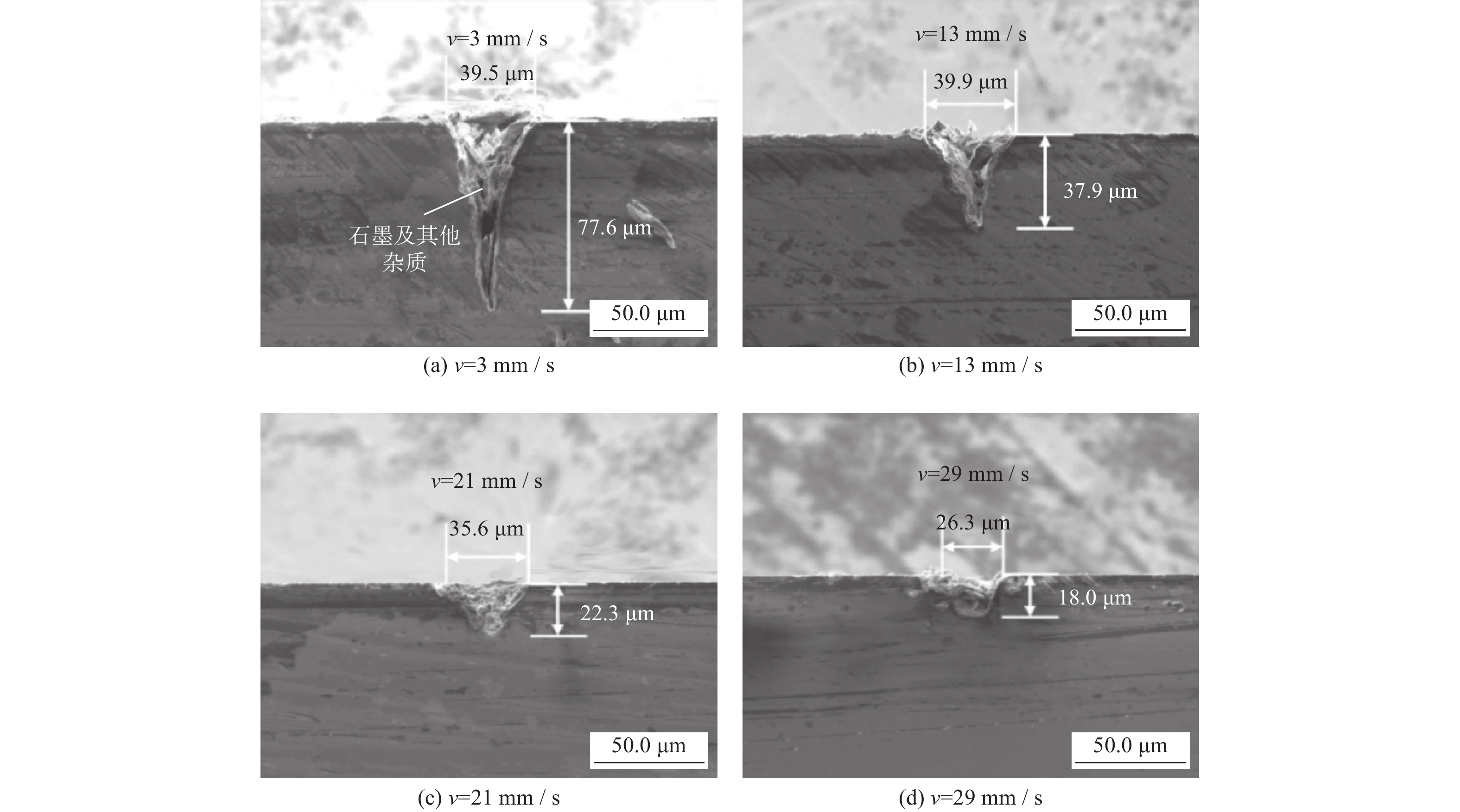
Objectives Chemical vapor deposition (CVD) diamond has excellent material properties and a wide range of application prospects, but due to its high hardness, brittleness and chemical inertness, microstructure processing on the surface and inside is extremely difficult. Based on the advantages of high precision, high efficiency and easy automation of laser processing, this paper adopts the ultraviolet nanosecond laser for CVD single diamond etching, and combines the laser line etching energy model with the basic research on the law of laser processing and etching principle. Methods A UV nanosecond laser is used to carry out basic research on the laws of laser processing and etching principle through the ablation threshold test, laser energy modeling and line etching test, scanning electron microscope observation and energy spectrum analysis test. The purpose of the ablation threshold test is to obtain a suitable range of processing parameters, set the laser scanning speed of 1 mm/s, the number of scans for 1 time, the laser repetition frequency range from 20 to 50 kHz with 10 kHz increment, and the laser power range from 1.2 to 12.0 W with 1.2 W increment, and observe the erosion situation by engraved lines. After obtaining a suitable range of processing parameters, a laser energy density model is established in which the main variables are laser power and scanning speed. Changes in the model are observed by varying different combinations of parameters, and the processing law is predicted and verified by combining with the actual line etching test. The test situation is mainly through the scanning electron microscope observation and record test data, one of the line etching groove of the internal and peripheral energy spectrum analysis, through the comparison of elemental changes and combined with the literature on the principle of ablation to carry out certain analysis. Results From the results of the ablation threshold test, when the laser repetition frequency is 20 kHz, the etching traces can be produced in the range of power 1.2-12.0 W, when the repetition frequency is 30 kHz, the etching traces start to be produced when the power is increased to 7.2 W, and when the repetition frequency is 40 and 50 kHz, the etching traces are not produced in the range of power 1.2-12.0 W, therefore, in order to obtain stable etching results, fixed the laser repetition frequency of 20 kHz in the subsequent line etching test. Therefore, in order to obtain stable etching results, the laser repetition frequency is fixed at 20 kHz in the subsequent line etching test, and the results of the line etching test can be seen from the side of the CVD diamond, the groove basically appears as a “V” shape, and in combination with the line etching model of the laser, the energy density of the laser shows a high distribution in the middle and low distribution around the edges, i.e., the center of the spot is high and the edges are low. Furthermore, the energy at the center of the spot is high, and the energy at the edge is low. In the one-factor test of power, when the power is 1.2, 3.0, 5.4, 10.8 W, the width of the line etching groove is 39.8, 39.8, 41.0, 38.8 μm, and the depth is 35.7, 41.1, 42.1, 57.2 μm, respectively, and the width and depth of the diamond line etching groove increase with the increase of the laser power. In the one-factor test of scanning speed, when the scanning speed is 3, 13, 21 and 29 mm/s, the widths of the wire-etched grooves are 39.5, 39.9, 35.6 and 26.3 μm, and the depths are 77.6, 37.9, 22.3 and 18.0 μm, and the widths as well as the depths of the grooves gradually decrease with the scanning speed increasing.The results of EDS analysis show that, compared with the unfinished area, the proportions of C elements in the grooves' interior, sidewalls and peripheral areas show a decrease in the proportion of C elements and an increase in the proportion of N and O elements compared to the unprocessed area, and they are nearly the same. Conclusions (1) Combined with the line etching energy model, the increase in power leads to an increase in the energy density of the laser, and at the same time, the peak energy increases, increasing the degree of ablation of the material, resulting in deepening the depth of the groove, in addition, when increasing the laser power, the height of the model increases more than the increase in the magnitude of the edges, and therefore it can be observed that the width and depth of the diamond line etching groove increases with the increase in laser power, but the impact on the depth is greater than the impact on the width phenomenon. Scanning speed increase leads to increase the spacing between individual laser pulses, the amount of superposition between the pulses and the superposition area decreases, making the energy at the superposition decreases, which leads to a reduction in the peak value of the energy at the superposition, in addition, the scanning speed increase also leads to the reduction of the number of laser pulses irradiated in the unit area, which, under the combined effect, reduces the depth of the wire etching groove. (2) EDS analysis shows that, compared with the unprocessed area, the C element content in the processed area is reduced, and the N and O element content is increased, so it can be initially judged that the mechanism of nanosecond laser processing of single-crystal diamond is the phase transformation of diamond at high temperatures, graphite oxidation, and sputtering of graphite and heterogeneous compounds. -
Key words:
- UV nanosecond laser /
- single crystal diamond /
- laser etching /
- flat top laser
-
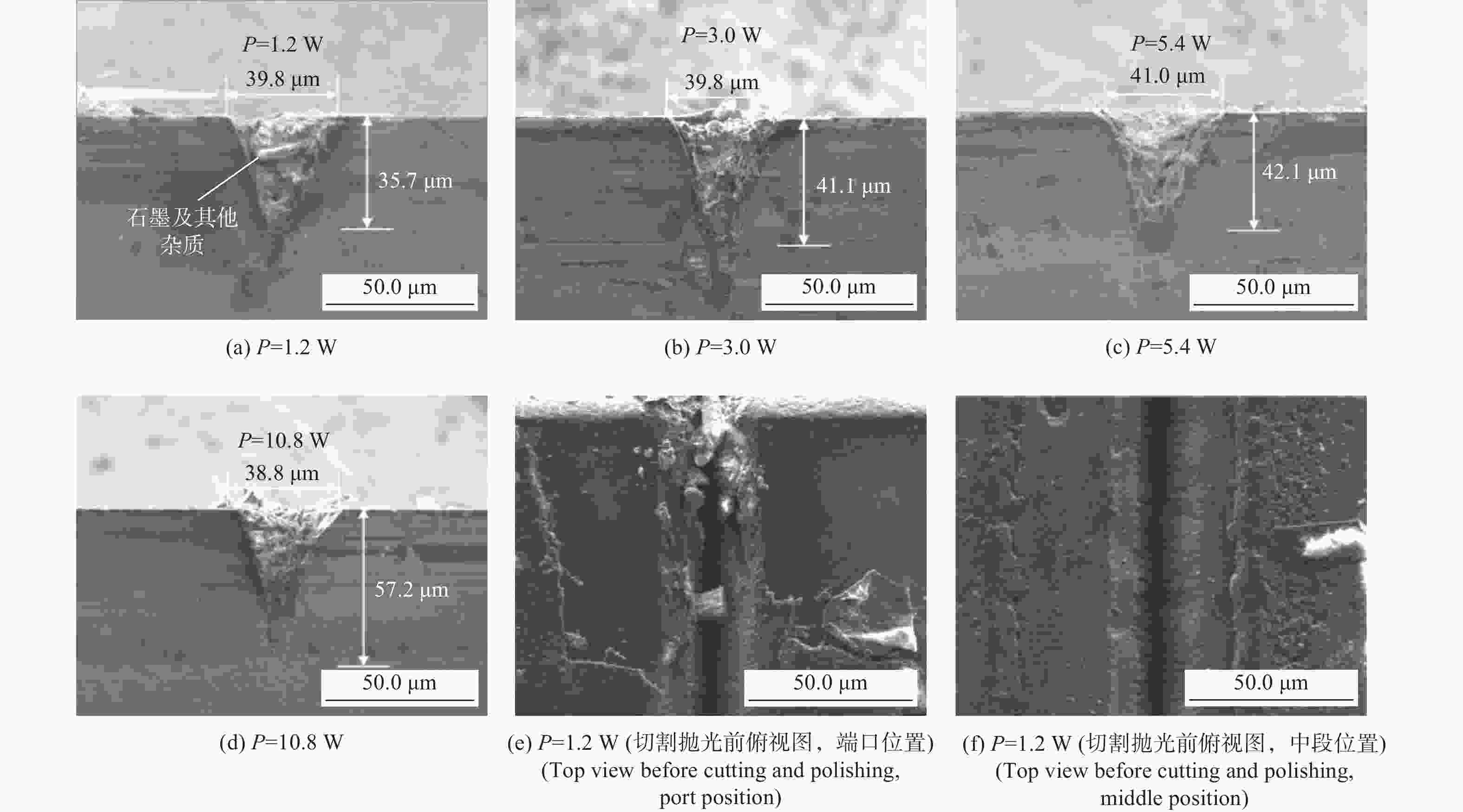
图 7 激光功率对线刻蚀槽宽度及深度的影响
Figure 7. Effect of laser power on line etching groove width and depth
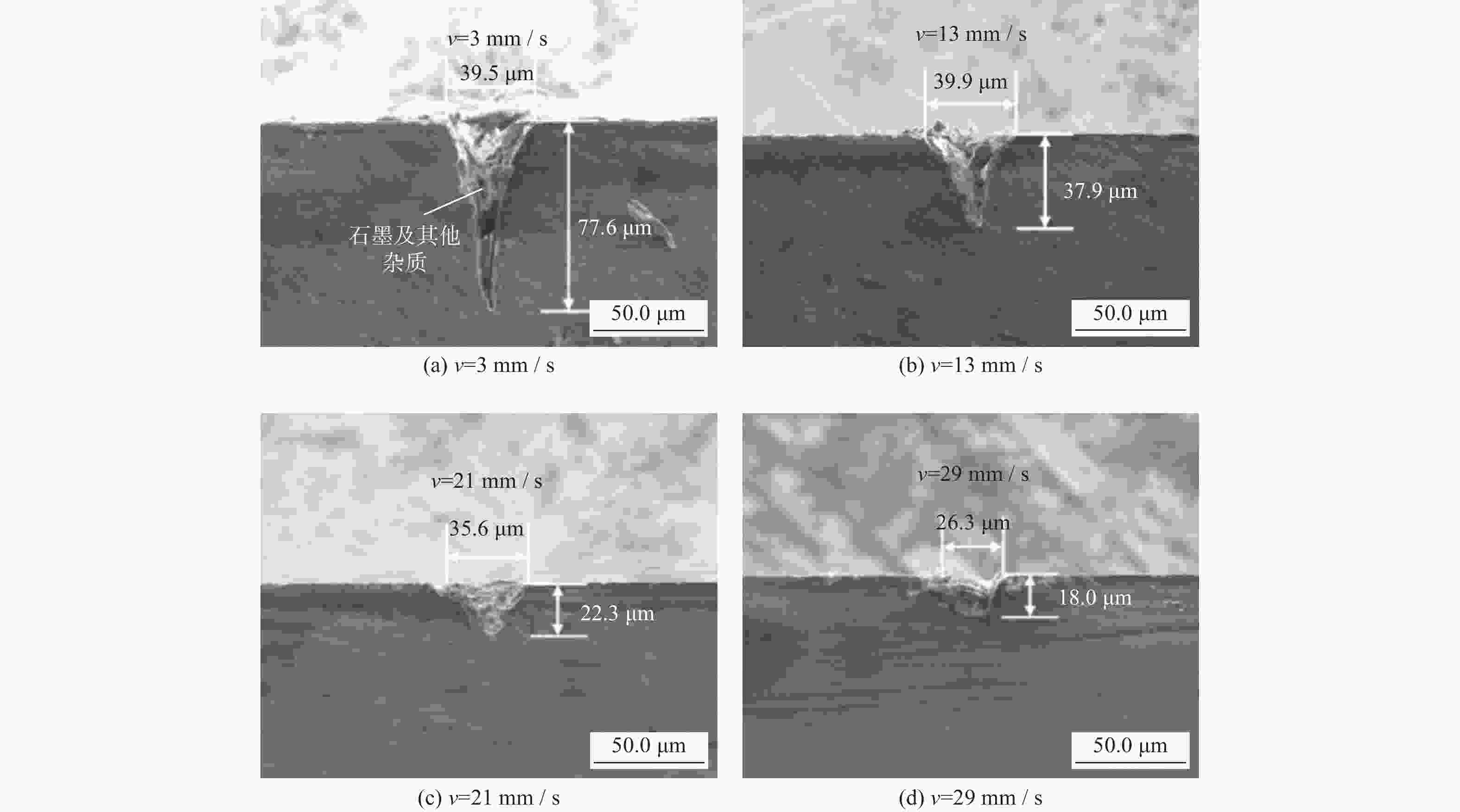
图 8 扫描速度对线刻蚀槽宽度及深度的影响
Figure 8. Effect of scanning speed on line etching groove width and depth
表 1 紫外纳秒激光参数
Table 1. UV nanosecond laser parameters
参数 数值或类型 波长 λ / nm 355 激光重复频率 f / kHz 20~200 光斑形状 方形 光斑边长 l / μm 20 脉冲持续时间 t / ns 15 最大功率 Pmax / W 12.0  下载: 导出CSV
表 2 线刻蚀试验参数
Table 2. Line etching experimental parameters
试验 激光功率 P / W 扫描速度 v / (mm·s−1) 扫描次数 n / 次 1 1.2, 3.0, 5.4, 10.8 1 1 2 3.0 3, 13, 21, 29 5
下载: 导出CSV
-
[1] 玄真武, 侯立, 王亨瑞, 等. 晶体院金刚石六十年研发 [J]. 人工晶体学报,2023,52(12):2094-2107. doi: 10.3969/j.issn.1000-985X.2023.12.004XUAN Zhenwu, HOU Li, WANG Hengrui, et al. Sixty years research of diamonds in Sinoma Snythetic Crystals Co. , Itd. [J]. Journal of Synthetic Crystals,2023,52(12):2094-2107. doi: 10.3969/j.issn.1000-985X.2023.12.004 [2] 李成明, 任飞桐, 邵思武, 等. 化学气相沉积(CVD)金刚石研究现状和发展趋势 [J]. 人工晶体学报,2022,51(5):759-780. doi: 10.3969/j.issn.1000-985X.2022.05.003LI Chengming, REN Feitong, SHAO Siwu, et al. Progress of chemical vapor deposition (CVD) diamond [J]. Journal of Synthetic Crystals,2022,51(5):759-780. doi: 10.3969/j.issn.1000-985X.2022.05.003 [3] LIANG Q, YAN C S, MENG Y F, et al. Recent advances in high-growth rate single-crystal CVD diamond [J]. Diamond and Related Materials,2009,18(5/6/7/8):698-703. doi: 10.1016/j.diamond.2008.12.002 [4] 王伟华, 贾怡, 李振, 等. 面向航天领域极端环境应用的金刚石材料及其器件 [J]. 硅酸盐学报,2024,52(5):1778-1788. doi: 10.14062/j.issn.0454-5648.20230688WANG Weihua, JIA Yi, LI Zhen, et al. Diamond materials and devices for extreme environment applications in aerospace [J]. Journal of the Chinese Ceramic Society,2024,52(5):1778-1788. doi: 10.14062/j.issn.0454-5648.20230688 [5] 吴俊, 马志斌, 沈武林. 氧回旋离子束刻蚀化学气相沉积金刚石膜 [J]. 强激光与粒子束,2012,24(10):2459-2463. doi: 10.3788/HPLPB20122410.2459WU Jun, MA Zhibin, SHEN Wulin. Etching of CVD diamond films using oxygen cyclotron ion beams [J]. High Power Laser and Particle Beams,2012,24(10):2459-2463. doi: 10.3788/HPLPB20122410.2459 [6] OKHOTNIKOV V V, LINNIK S A, GAYDAYCHUK A V. The research of diamond coatings morphology evolution under the action of reactive ion etching in perpendicular direction [J]. Key Engineering Materials,2016,712:87-92. doi: 10.4028/www.scientific.net/KEM.712.87 [7] 叶盛, 赵上熳, 邢忠福, 等. 激光技术在金刚石加工中的研究及应用进展 [J]. 红外与激光工程,2024,53(2):44-65. doi: 10.3788/IRLA20230567YE Sheng, ZHAO Shangman, XING Zhongfu, et al. Research and application progress of laser technology in diamond processing [J]. Infrared and Laser Engineering,2024,53(2):44-65. doi: 10.3788/IRLA20230567 [8] 汪晖, 温秋玲, 黄辉, 等. 飞秒激光加工CVD单晶金刚石的烧蚀特征和机理研究 [J]. 光子学报,2023,52(12):51-65. doi: 10.3788/gzxb20235212.1214001WANG Hui, WEN Qiuling, HUANG Hui, et al. Ablation characteristics and material removal mechanism of CVD single crystal diamond under femtosecond laser irradiation [J]. Acta Photonica Sinica,2023,52(12):51-65. doi: 10.3788/gzxb20235212.1214001 [9] 温秋玲, 韦新宇, 王华禄, 等. 皮秒激光加工CVD单晶金刚石的特征和机理研究 [J]. 光子学报,2021,50(6):126-136. doi: 10.3788/gzxb20215006.0650113WEN Qiuling, WEI Xinyu, WANG Hualu, et al. Characteristics and mechanism of CVD single crystal diamond processed by picosecond laser [J]. Acta Photonica Sinica,2021,50(6):126-136. doi: 10.3788/gzxb20215006.0650113 [10] EBERLE G, WEGENER K. Ablation study of WC and PCD composites using 10 picosecond and 1 nanosecond pulse durations at green and infrared wavelengths [J]. Physics Procedia,2014,56:951-962. doi: 10.1016/j.phpro.2014.08.115 [11] OGAWA Y, OTA M, NAKAMOTO K, et al. A study on machining of binder-less polycrystalline diamond by femtosecond pulsed laser for fabrication of micro milling tools [J]. CIRP Annals,2016,65(1):245-248. doi: 10.1016/j.cirp.2016.04.081 [12] KONONENKO V V, KONONENKO T V, PIMENOV S M, et al. Effect of the pulse duration on graphitisation of diamond during laser ablation [J]. Quantum Electronics,2005,35(3):252-256. doi: 10.1070/QE2005v035n03ABEH002900 [13] 陈妮, 闫博, 李振军, 等. 基于高斯脉冲的激光刻蚀CVD金刚石研究 [J]. 中国激光,2020,47(12):127-134. doi: 10.3788/CJL202047.1202007CHEN Ni, YAN Bo, LI Zhenjun, et al. Gaussian pulsed laser etching of CVD diamonds [J]. Chinese Journal of Lasers,2020,47(12):127-134. doi: 10.3788/CJL202047.1202007 [14] ZHANG Z, ZHANG Q L, WANG Q W, et al. Investigation on the material removal behavior of single crystal diamond by infrared nanosecond pulsed laser ablation [J]. Optics & Laser Technology,2020,126:106086. doi: 10.1016/j.optlastec.2020.106086 [15] 俞君, 曾智江, 朱三根, 等. 紫外激光在微细加工技术中的优势研究 [J]. 红外,2008,29(6):9-13,40. doi: 10.3969/j.issn.1672-8785.2008.06.003YU Jun, ZENG Zhijiang, ZHU Sangen, et al. Research on advantages of UV laser in fine processing technology [J]. Infrared,2008,29(6):9-13,40. doi: 10.3969/j.issn.1672-8785.2008.06.003 [16] 王孟洁, 王菲, 张承双, 等. 平顶激光辐照CF/PEEK复合材料熔凝过程有限元仿真 [J]. 激光与光电子学进展,2023,60(13):257-263. doi: 10.3788/LOP230510WANG Mengjie, WANG Fei, ZHANG Chengshuang, et al. Study on melting kinetics of CF/PEEK composites irradiated by flat top laser [J]. Laser & Optoelectronics Progress,2023,60(13):257-263. doi: 10.3788/LOP230510 [17] 明兴祖, 马玉龙, 贾松权, 等. 能量耦合模型的飞秒激光烧蚀面齿轮形貌研究 [J]. 激光与红外,2023,53(1):41-50. doi: 10.3969/j.issn.1001-5078.2023.01.006MING Xingzu, MA Yulong, JIA Songquan, et al. Research on surface gear topography of femtosecond laser ablation based on energy coupling model [J]. Laser & Infrared,2023,53(1):41-50. doi: 10.3969/j.issn.1001-5078.2023.01.006 [18] MOUHAMADALI F, EQUIS S, SAEIDI F, et al. Nanosecond pulsed laser-processing of CVD diamond [J]. Optics and Lasers in Engineering,2020,126:105917. doi: 10.1016/j.optlaseng.2019.105917 [19] 韦新宇, 温秋玲, 陆静, 等. 紫外纳秒激光加工金刚石微槽工艺参数优化研究 [J]. 中国激光,2022,49(10):96-106. doi: 10.3788/CJL202249.1002406WEI Xinyu, WEN Qiuling, LU Jing, et al. Research on parameters optimization of diamond microgrooves processed by ultravilot nanosecond laser [J]. Chinese Journal of Lasers,2022,49(10):96-106. doi: 10.3788/CJL202249.1002406 [20] 王华禄. 纳秒/皮秒激光烧蚀单晶金刚石材料的微观特征及去除机理研究[D]. 厦门: 华侨大学, 2021.WANG Hualu. Study on the micro-characteristics and the material removal mechanism of single-crystal diamond ablated by nanosecond and picosecond laser [D]. Xiamen: Huaqiao University, 2021. -

 点击查看大图
计量
- 文章访问数: 125
- HTML全文浏览量: 63
- PDF下载量: 13
- 被引次数: 0
 邮件订阅
邮件订阅 RSS
RSS