Highly efficient polishing of polycrystalline CVD diamond via atmosphere inductively coupled plasma
-
摘要: 作为一种典型的难加工材料,多晶金刚石的抛光存在着材料去除率低、损伤引入较多、难以获得亚纳米级粗糙度等诸多问题。采用一种基于大气电感耦合等离子体的非接触式加工方法,在纯氩等离子体中引入氧气作为反应气,激发产生高活性氧自由基,并在多晶金刚石表面不同位点处发生差异化刻蚀,最终实现多晶金刚石的高效抛光。研究结果表明:随着含氧等离子体辐照的进行,多晶金刚石表面晶粒尖端位点被快速去除,晶粒间的高度差大幅下降,且金刚石表面粗糙度Sa在30 min内从10.10 μm降低至93.70 nm,材料去除率可达34.4 μm/min,远高于传统的机械或化学机械抛光方法。拉曼光谱与X射线衍射谱分析表明,该抛光方法未引入非晶碳或新应力损伤,不改变多晶金刚石表面晶粒取向。该方法可作为一种多晶金刚石粗抛技术,与化学机械抛光、紫外激发抛光等精抛工艺相结合,显著提升多晶金刚石的综合抛光效率。
-
关键词:
- 多晶金刚石 /
- 高效抛光 /
- 大气电感耦合等离子体 /
- 高活性氧自由基
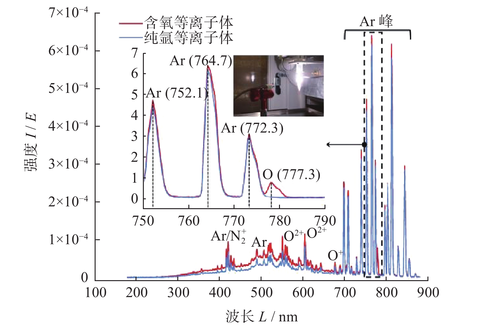
Abstract: Objectives: As a typical difficult-to-machine material, polycrystalline CVD diamond often requires sophisticated and time-consuming polishing methods to achieve a smooth surface. In this study, a non-contact polishing method based on atmospheric inductively coupled plasma is investigated for the polishing of polycrystalline CVD diamond. Several indicators, including surface roughness, surface chemical composition, inner crystal structure, and material removal rate (MRR), are measured during the polishing process to evaluate the surface quality and polishing efficiency. Methods: The atmospheric inductively coupled plasma device, consisting of a plasma working zone, radio frequency (RF) power, electric sparker, RF match, mass flow controller, and water cooler, is used for polishing experiments. Oxygen is used as a reaction gas and added to the pure argon plasma, generating highly active oxygen radicals. The polycrystalline CVD diamond sample is fully exposed to oxygen-containing plasma irradiation to gain sufficient activation energy and react with the oxygen radicals. Once the processing is completed, the RF power is turned off, the oxygen supply is stopped, and the diamond is raised and cooled with pure argon shielding to protect the sample from being etched by ambient oxygen at high temperatures. Laser scanning confocal microscopy and scanning electron microscopy (SEM) are used to observe the diamond morphology, while the Sa roughness at different scales is characterized by scanning white interferometry and atomic force microscopy (AFM). The material removal rate is measured using an ultra-precision balance, and surface temperature is detected by an infrared imager. Raman spectroscopy and X-ray diffraction (XRD) are separately used to characterize the surface chemical composition and crystal orientation of the diamond before and after polishing. Results: The results of diamond treatment under different plasma irradiation conditions show that pure argon plasma tends to deteriorate the surface quality, while oxygen-containing plasma achieves significant polishing performance, removing grain tips and protruding structures. The morphology evolution of diamonds during the polishing process reveals that the initial surface is extremely rough, with severe surface irregularities and angular grain structures. After exposure to oxygen-containing plasma, the elevated grain structures are gradually removed, and the sharp edges are rounded. As the plasma irradiation time increases, some protruding sites are further eliminated, revealing the remaining cavities formed during the crystal growth process. Ultimately, the various crystal grains on the diamond surface maintain a consistent height, forming a relatively smooth surface. The fluctuating grain boundaries, which are widespread among the crystal grains, inhibit the formation of a smoother surface. The polishing effect can be explained by the principle of plasma-based atom-selective etching (PASE). During the polishing process, carbon atoms with different bonding states are randomly distributed on the diamond surface. Among them, carbon atoms at the grain tips, which only bond with atoms below and possess less stable bonds compared to those in the substrate, have lower activation energy. Consequently, tip carbon atoms preferentially react with active oxygen radicals due to their lower activation energy, accounting for the removal of grain tips during the initial polishing stage. As the polishing process continues, carbon atoms with fewer covalent bonds fade away, and the bonding states become equivalent in local areas, contributing to a progressively smoother surface. However, carbon atoms at the crystal boundary zones have complex arrangements and bonding characteristics, which restrict the differential removal of carbon atoms and hinder the overall polishing effect. The roughness evolution results show that the final Sa roughness of polycrystalline CVD diamond is reduced to 93.70 nm over a 400 μm × 400 μm area and 21.40 nm over a 20 μm × 20 μm area after polishing for 30 minutes. In some smooth areas, the roughness is as low as 2.53 nm, while in the crystal boundary zones, it reaches 31.30 nm. The presence of the crystal boundary zone hinders the global polishing performance. After 30 minutes of polishing, the surface roughness stabilizes, with the MRR also stabilizing at 34.4 μm/min. Surface composition analysis indicates a tensile stress of 1.5309 GPa on the diamond surface, and the polishing process dose not introduce new stress or amorphous carbon contaminants. XRD spectra show that there is no change in the crystal grain orientation of the diamond before and after polishing, demonstrating that PASE acts on all crystal planes of polycrystalline diamond (PCD) without preference for any specific crystal plane. Conclusions: Atmospheric inductively coupled plasma (ICP) can be used to efficiently smooth polycrystalline CVD diamond based on the principle of PASE. During the polishing process, oxygen is introduced as a reaction gas, generating oxygen radicals that selectively etch the diamond by preferentially removing carbon atoms with low activation energy, thus rapidly smoothing the surface. The Sa roughness of diamond is reduced from 10.10 μm (400 μm × 400 μm) and 338.00 nm (20 μm × 20 μm) to 93.70 nm and 21.40 nm, respectively, after 30 minutes of polishing. As polishing progresses, the MRR sharply decreases and eventually stabilizes at around 34.4 μm/min. The surface chemical composition and crystal grain orientation of polycrystalline CVD diamond remain consistent before and after polishing. Overall, atmospheric ICP can be an efficient pre-polishing method to significantly improve the overall polishing efficiency of polycrystalline CVD diamond. -
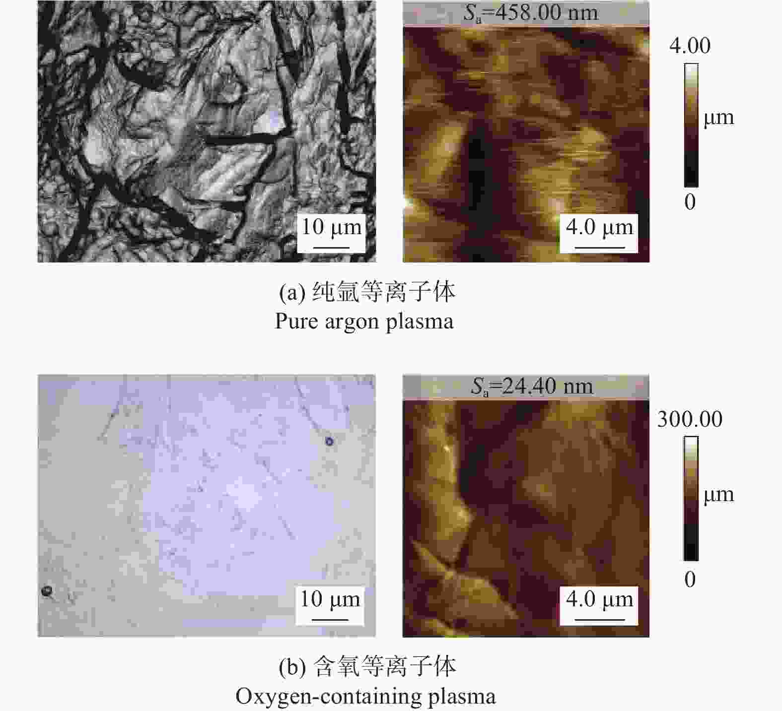
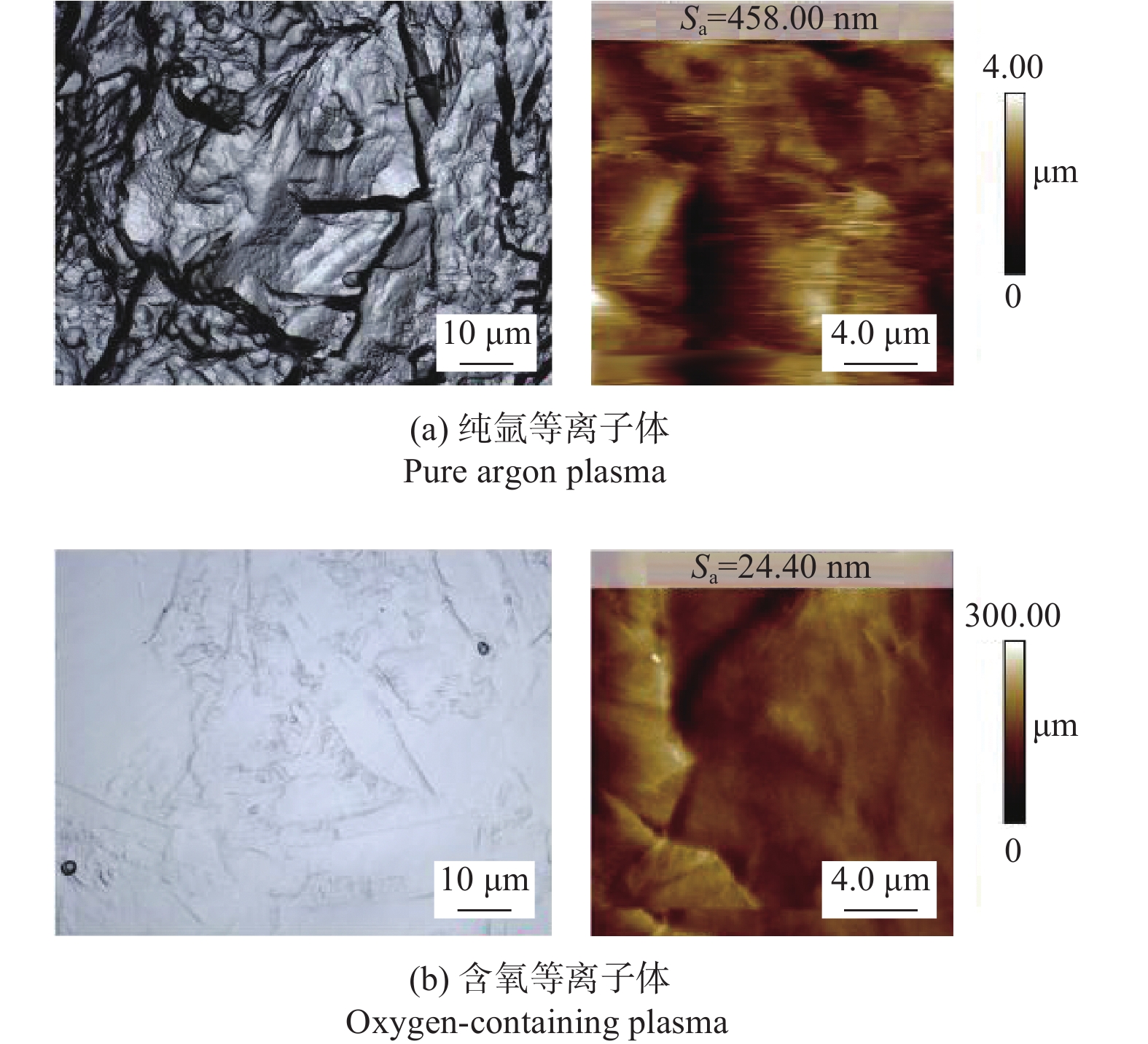
图 4 不同等离子体辐照处理20 min结果
Figure 4. 20 min treatment effect of polycrystalline diamond under radiation of different plasmas
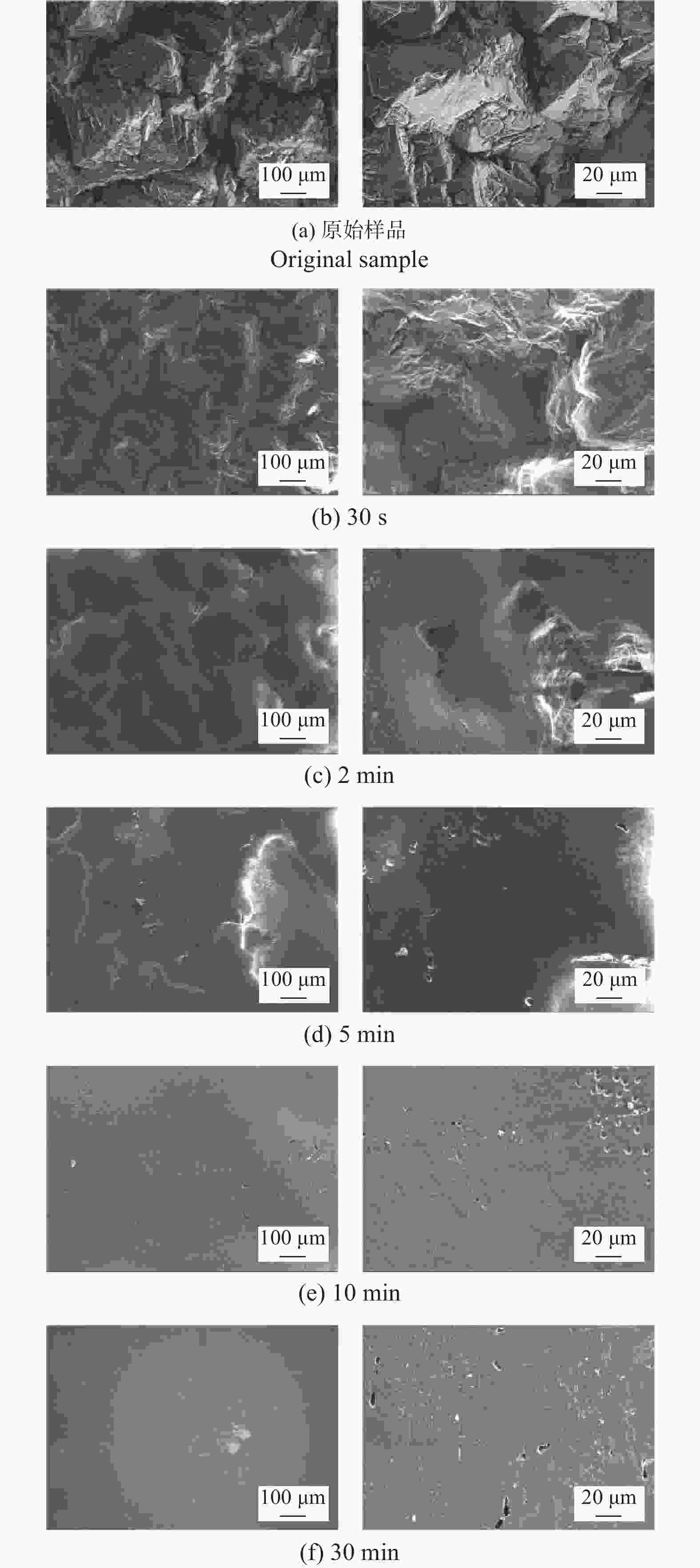
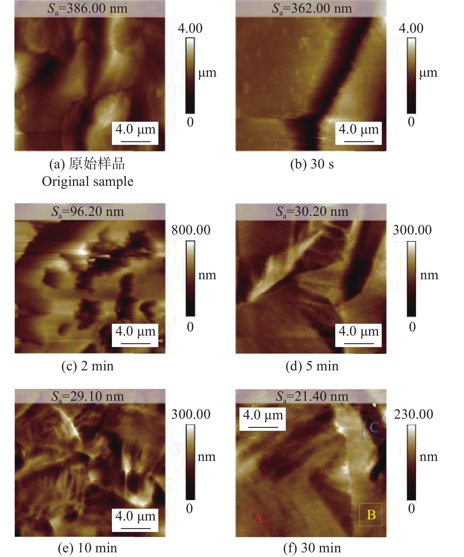
图 5 多晶金刚石表面形貌随抛光时间变化的结果
Figure 5. Morphology of polycrystalline diamond under different polishing durations
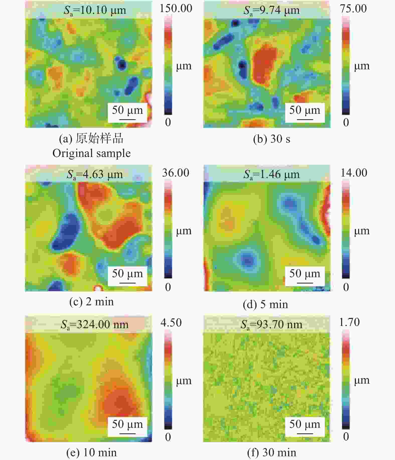
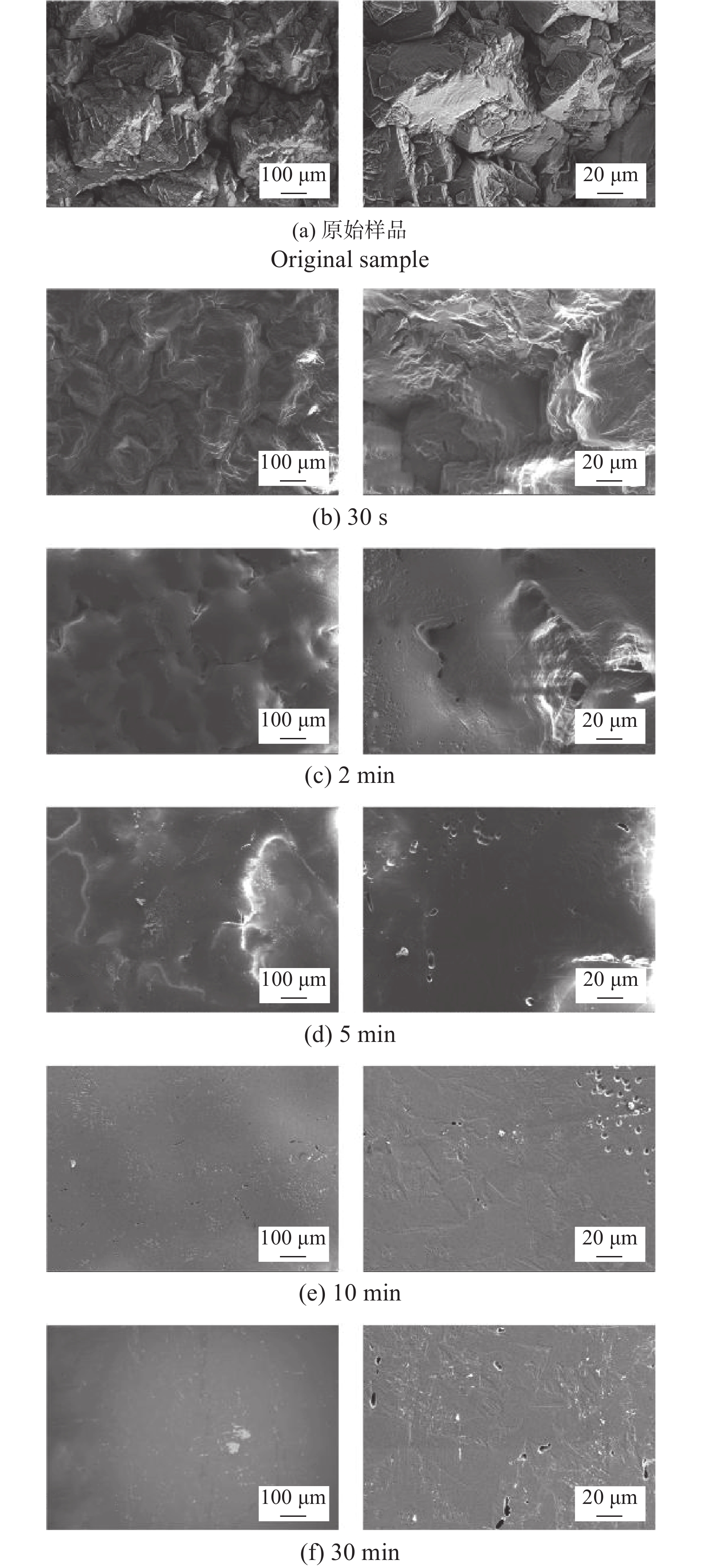
图 6 抛光过程中多晶金刚石表面大尺度范围内形貌演变
Figure 6. Morphological evolution of polycrystalline diamond at large scale during polishing
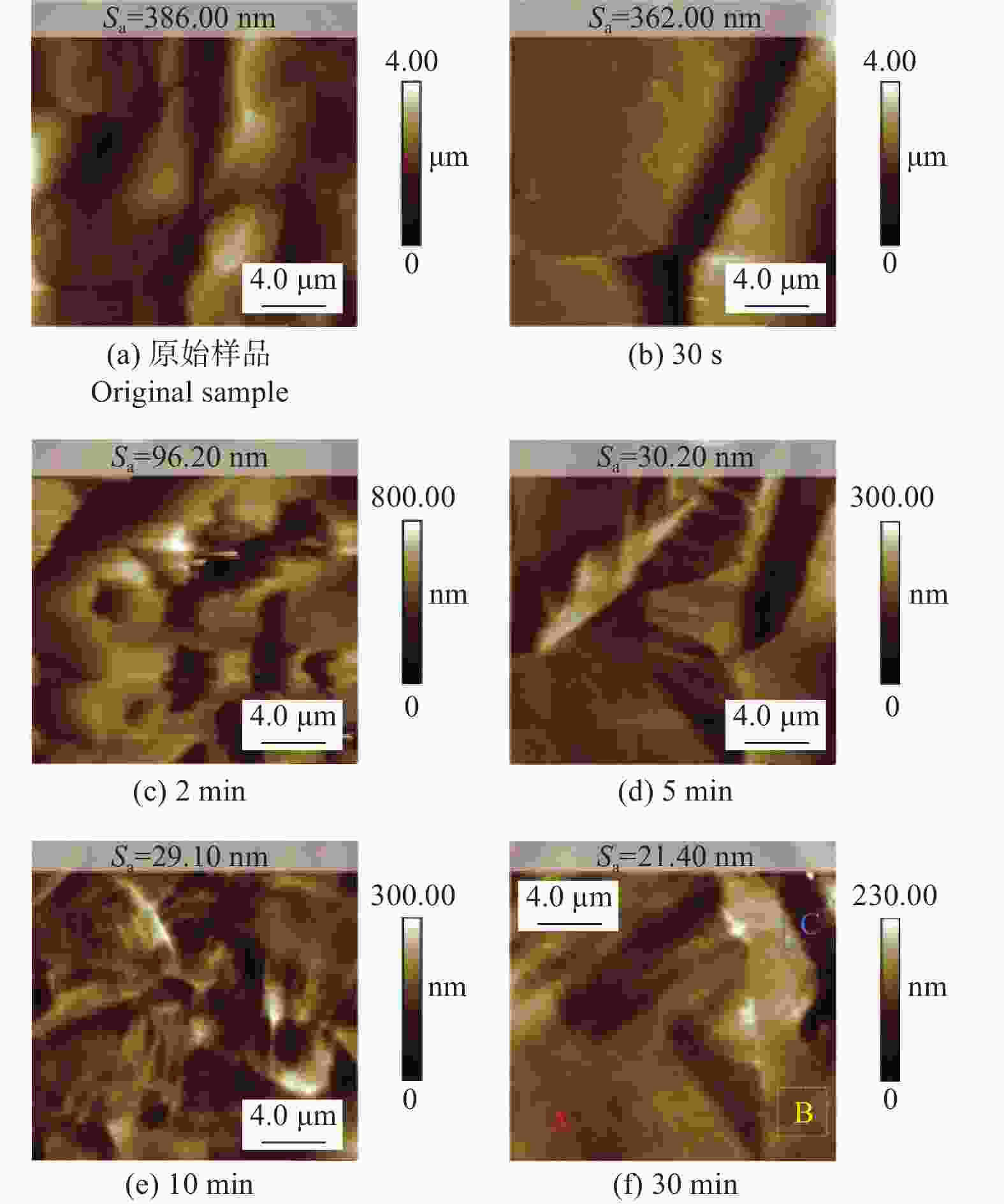
图 7 抛光过程中多晶金刚石表面小尺度范围内形貌演变
Figure 7. Morphological evolution of polycrystalline diamond at small scale during polishing
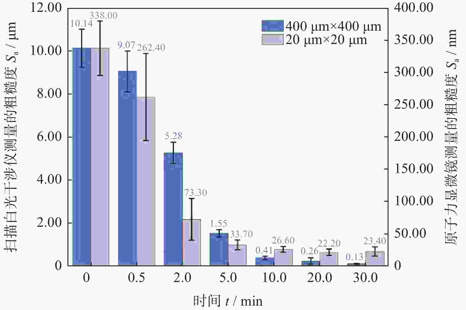
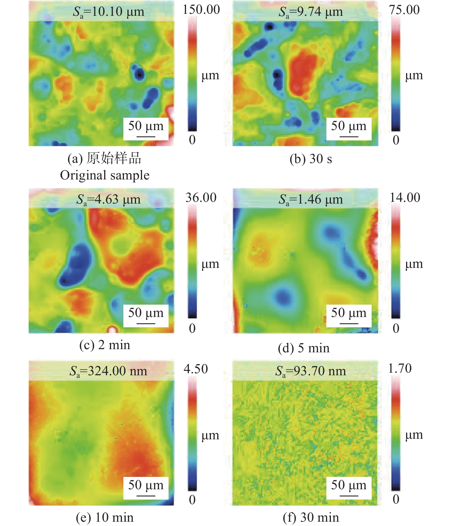
图 8 抛光过程中多晶金刚石表面不同范围内粗糙度Sa演变
Figure 8. Roughness Sa evolution of polycrystalline diamond at different scale during polishing
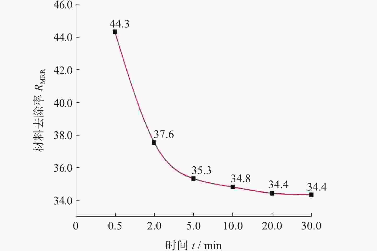
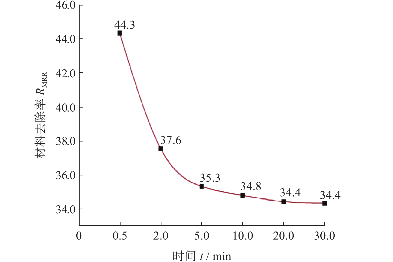
图 9 抛光过程中多晶金刚石材料去除率变化
Figure 9. Variation of material removal rate of polycrystalline diamond during polishing

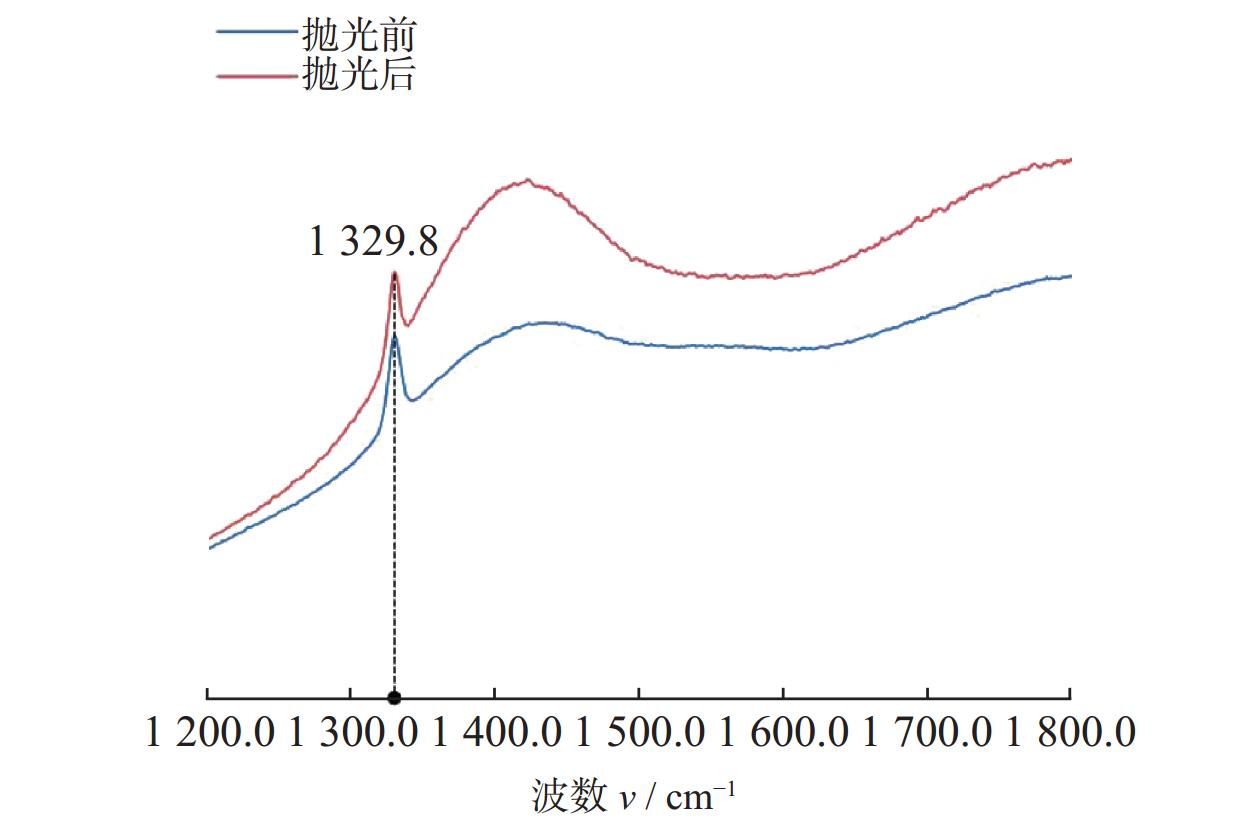
图 10 多晶金刚石抛光前后拉曼光谱
Figure 10. Raman spectra of polycrystalline diamond before and after polishing
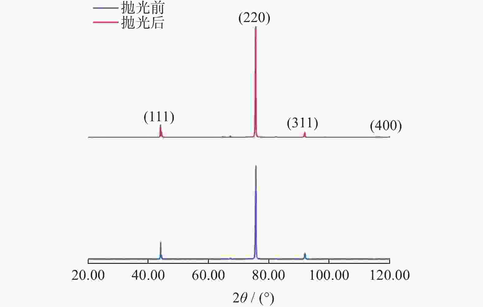
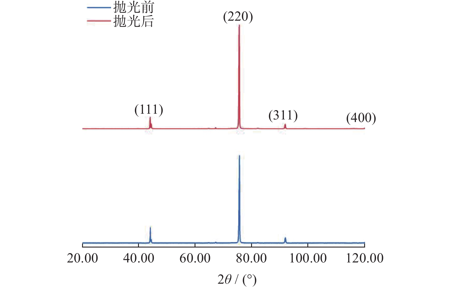
图 11 多晶金刚石抛光前后X射线衍射谱图
Figure 11. X-ray diffraction spectra of polycrystalline diamond before and after polishing
表 1 实验参数
Table 1. Experimental parameters
实验参数 具体条件 玻璃炬管直径 d /mm 内炬管(内直径/外直径):14/16
外炬管(内直径/外直径):18/20射频电源功率 Q /W 1200 射频电源频率 f /MHz 27.12 载流气流速 v1 /slm 1.5 冷却气流速 v2 /slm 18 反应气流速 v3 /sccm 60 工作距离 l /mm 15  下载: 导出CSV
-
[1] 李明吉. 大尺寸高质量金刚石厚膜制备及氮掺杂对金刚石膜生长的影响研究 [D]. 长春: 吉林大学, 2006.LI Mingji. Preparation of large-sized high-quality diamond thick films, and influence of nitrogen doping on the growth of diamond films [D]. Changchun: Jilin University, 2006. [2] UMEZAWA H. Recent advances in diamond power semiconductor devices [J]. Materials Science in Semiconductor Processing,2018,78:147-156. doi: 10.1016/j.mssp.2018.01.007 [3] MOLLART T P, WORT C J H, PICKLES C S J, et al. CVD diamond optical components, multispectral properties, and performance at elevated temperatures [J]. Proceeding SPIE,2001,4375: 180-198. doi: 10.1117/12.439175 [4] 苑泽伟. 利用化学和机械协同作用的CVD金刚石抛光机理与技术 [D]. 大连: 大连理工大学, 2012.YUAN Zewei. Mechanism and technology for polishing CVD diamond with chemical and mechanical synergistic effects [D]. Dalian: Dalian University of Technology, 2012. [5] PHUNG H M, TATAR-MATHES P, ROGERS A, et al. Thermal behavior and power scaling potential of membrane external-cavity surface-emitting lasers (MECSELs) [J]. IEEE Journal of Quantum Electronics,2022,58(2):1-11. doi: 10.1109/JQE.2022.3147482 [6] LIAO M Y. Progress in semiconductor diamond photodetectors and MEMS sensors [J]. Functional Diamond,2021,1(1):29-46. doi: 10.1080/26941112.2021.1877019 [7] 王伟华, 代兵, 王杨, 等. 金刚石光学窗口相关元件的研究进展 [J]. 材料科学与工艺,2020,28(3):42-57. doi: 10.11951/j.issn.1005-0299.20200074WANG Weihua, DAI Bing, WANG Yang, et al. Recent progress of diamond optical window-related components [J]. Material Science and Technology,2020,28(3):42-57. doi: 10.11951/j.issn.1005-0299.20200074 [8] SONG X, WANG H, WANG X C, et al. Fabrication and evaluation of diamond thick film-Si3N4 brazed cutting tool by microwave plasma chemical vapor deposition method [J]. Journal of Materials Processing Technology,2021,291:117034. doi: 10.1016/j.jmatprotec.2020.117034 [9] 吕智, 马忠强, 蒋燕麟, 等. 功能金刚石的发展现状及产业化前景 [J]. 超硬材料工程,2020,32(4):22-34. doi: 10.3969/j.issn.1673-1433.2020.04.006LV Zhi, MA Zhongqiang, JIANG Yanlin, et al. The development status and industrialization prospect of functional diamond [J]. Superhard Material Engineering,2020,32(4):22-34. doi: 10.3969/j.issn.1673-1433.2020.04.006 [10] MALSHE A P, PARK B S, BROWN W D, et al. A review of techniques for polishing and planarizing chemically vapor-deposited (CVD) diamond films and substrates [J]. Diamond and Related Materials,1999,8:1198-1213. doi: 10.1016/S0925-9635(99)00088-6 [11] KABOLI S, BURNLEY P C. Direct observations of crystal defects in polycrystalline diamond [J]. Materials Characterization,2018,142:154-161. doi: 10.1016/j.matchar.2018.05.036 [12] XIAO C, HSIA F C, SUTTON-COOK A, et al. Polishing of polycrystalline diamond using synergies between chemical and mechanical inputs: A review of mechanisms and processes [J]. Carbon,2022,196:29-48. doi: 10.1016/j.carbon.2022.04.028 [13] MANDAL S, THOMAS E L H, GINES L, et al. Redox agent enhanced chemical mechanical polishing of thin film diamond [J]. Carbon,2018,130:25-30. doi: 10.1016/j.carbon.2017.12.077 [14] THOMAS E L H, NELSON G W, MANDAL S, et al. Chemical mechanical polishing of thin film diamond [J]. Carbon,2014,68:473-479. doi: 10.1016/j.carbon.2013.11.023 [15] WATANABE J J, TOUGE M, SAKAMOTO T. Ultraviolet-irradiated precision polishing of diamond and its related materials [J]. Diamond and Related Materials,2013,39:14-19. doi: 10.1016/j.diamond.2013.07.001 [16] LIANG Y F, ZHENG Y T, WEI J J, et al. Effect of grain boundary on polycrystalline diamond polishing by high-speed dynamic friction [J]. Diamond and Related Materials,2021,117:108461. doi: 10.1016/j.diamond.2021.108461 [17] LU Y X, WANG B, MU Q, et al. Nanoscale smooth and damage-free polycrystalline diamond surface ground by coarse diamond grinding wheel [J]. Diamond and Related Materials,2022,125:108971. doi: 10.1016/j.diamond.2022.108971 [18] OGAWA Y, OTA M, NAKAMOTO K, et al. A study on machining of binder-less polycrystalline diamond by femtosecond pulsed laser for fabrication of micro milling tools [J]. CIRP Annals,2016,65:245-248. doi: 10.1016/j.cirp.2016.04.081 [19] RALCHENKO V G, ASHKINAZI E E, ZVEDEEV E V, et al. High-rate ultrasonic polishing of polycrystalline diamond films [J]. Diamond and Related Materials,2016,66:171-176. doi: 10.1016/j.diamond.2016.05.002 [20] 张翊, 吴兵, 张临风, 等. 面向原子级表面制造的等离子体诱导原子选择刻蚀技术 [J]. 中国科学: 技术科学,2022,52(6):882-892. doi: 10.1360/SST-2021-0584ZHANG Yi, WU Bing, ZHANG Linfeng, et al. Atomic surface manufacturing based on plasma-induced atom-selective etching [J]. Scientia Sinica(Technologica),2022,52(6):882-892. doi: 10.1360/SST-2021-0584 [21] LIU W, XIAO Y X, ZHANG Y J, et al. Highly efficient and atomic-scale smoothing of single crystal diamond through plasma-based atom-selective etching [J]. Diamond and Related Materials,2024,143:110840. doi: 10.1016/j.diamond.2024.110840 [22] RALCHENKO V G, SMOLIN A A, PEREVERZEV V G, et al. Diamond deposition on steel with CVD tungsten intermediate layer [J]. Diamond and Related Materials,1995,4:754-758. doi: 10.1016/0925-9635(94)05299-9 [23] VERES M, KOÓS M, TÓTH S, et al. Sp2 carbon defects in nanocrystalline diamond detected by Raman spectroscopy [J]. IOP Conference Series: Materials Science and Engineering,2010,15(1):012023. doi: 10.1088/1757-899X/15/1/012023 [24] 朱瑞华, 刘金龙, 陈良贤, 等. 金刚石自支撑膜拉曼光谱1420 cm−1特征峰研究 [J]. 人工晶体学报,2015,44(4):867-871. doi: 10.3969/j.issn.1000-985X.2015.04.003ZHU Ruihua, LIU Jinlong, CHEN Liangxian, et al. Research on 1420 cm−1 characteristic peak of free-standing diamond films in Raman spectrum [J]. Journal of Synthetic Crystals,2015,44(4):867-871. doi: 10.3969/j.issn.1000-985X.2015.04.003 [25] JIANG M, LI L, SUN X M, et al. Research on the mechanism and process of polycrystalline diamond by EDM [J]. The International Journal of Advanced Manufacturing Technology,2023,125:819-830. doi: 10.1007/s00170-022-10770-7 [26] CHEN K, TAO T, HU W X, et al. High-speed growth of high-quality polycrystalline diamond films by MPCVD [J]. Carbon Letters,2023,33:2003-2010. doi: 10.1007/s42823-023-00534-y -


 点击查看大图
计量
- 文章访问数: 1315
- HTML全文浏览量: 563
- PDF下载量: 137
- 被引次数: 0
 邮件订阅
邮件订阅 RSS
RSS