Effect of doped elements X (B, Al, Sn, Co) on binding performance of IDB-X/Diamond interface
-
摘要: 基于量子力学第一性原理,建立了IDB-B/Diamond、IDB-Al/Diamond、IDB-Sn/Diamond和IDB-Co/Diamond 4种膜基界面模型,计算了膜基界面结合能、差分电荷密度和布居数,以探究孕镶金刚石钻头(impregnated diamond bits, IDB)基体中的常用元素X(X = B、Al、Sn、Co)对 IDB-X/Diamond膜基结合强度的影响机制。计算结果表明:膜基界面结合能大小为Wad-B > Wad-Al > Wad-Co > Wad-Sn;B、Al是增强膜基结合强度的有益元素,因为B、Al原子的电荷主要转移到掺杂位点附近的C1~C3原子,其与C1~C3原子的键合作用强;Sn、Co会削弱膜基结合强度,这是由于Sn、Co原子与C1~C3原子的键合作用弱,同时膜基界面间的其他C原子因俘获电荷而相斥。压痕对比的实验结果与仿真结论相符。Abstract:
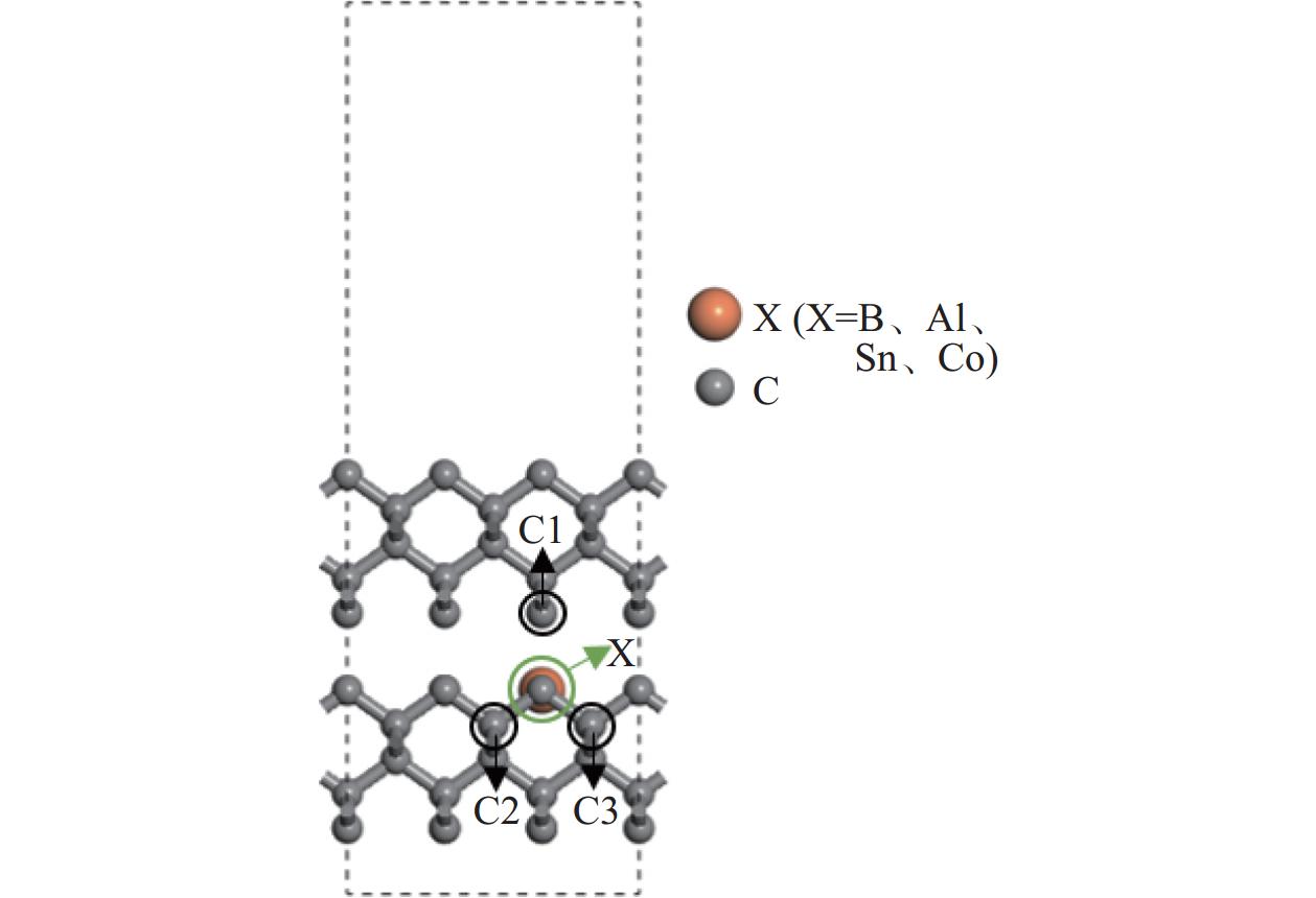
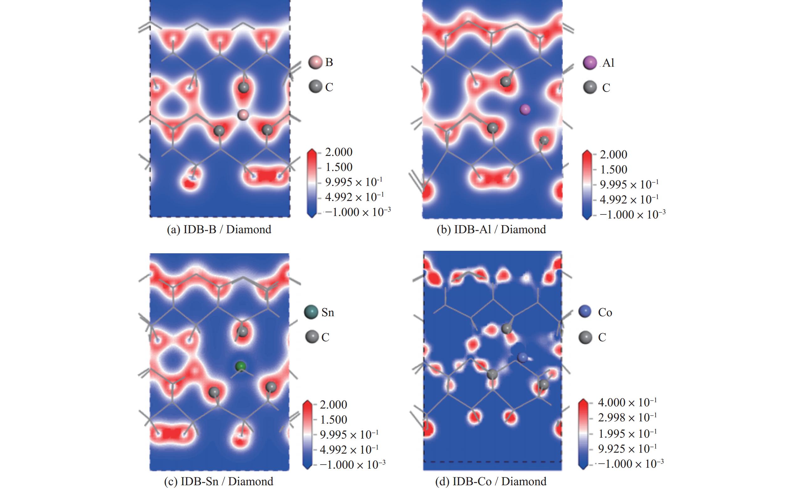
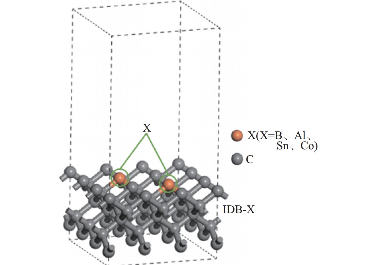
Objectives At present, resource exploration and mining continue to expand to deep underground. Impregnated diamond bits (IDB) with excellent performance have become the main tool for deep underground drilling. Our research group has found that depositing a layer of CVD diamond coating in situ on the surface of IDB can achieve homogeneous epitaxial growth and heterogeneous epitaxial growth of diamond coatings, which can improve the working life of IDB. This article is based on the first principles of quantum mechanics and uses the CASTEP computational tool to study the influence mechanism of X (X = B, Al, Sn, Co) elements commonly used in the IDB on the interfacial bonding performance of CVD diamond coatings on IDB from a microscopic perspective. It provides a theoretical reference and basis for further optimizing the formulation of drill bit substrates and improving the interfacial bonding strength between the film and substrate. Methods This article uses the CASTEP module of the quantum mechanics computing software Materials Studio to study the influence mechanism of X (X = B, Al, Sn, Co) elements commonly used in IDB on the interfacial bonding performance of CVD diamond coatings on IDB from a microscopic perspective. Firstly, establish [100] crystal orientation, 3×3 size IDB, and CVD diamond coating supercell models, with dimensions of 7.54 Å × 7.54 Å × 3.56 Å along the X, Y, and Z directions. After adding a vacuum layer with a thickness of 12 Å, the IDB model and CVD diamond coating model are obtained. Then, replace the C atoms at specific locations on the surface of the IDB model with X (X = B, Al, Sn, Co) atoms. Afterwards, the IDB-X substrate is combined with the CVD diamond coating model along the [100] crystal plane to establish an IDB-X/Diamond film substrate interface model. After testing, the film-substrate interface spacing is set to 2 Å. Next, the CASTEP module is used to optimize the IDB-X/Diamond film-substrate interface model doped with X (X = B, Al, Sn, Co) atoms. The properties of the four film-substrate interface models are analyzed from the aspects of film-substrate interface binding energy, differential charge density, and Mulliken population. Finally, verification is conducted with indentation experiments. Results (1) From the perspective of film-substrate interface binding energy, the binding energies of B, Al, Co, and Sn atom doping are 11.68, 9.94, 7.38, and 6.85 J/m2, respectively. Based on the weakening phase Co of the film-substrate interface binding energy, the film-substrate interface binding energy doped with B and Al atoms is significantly higher than that of Co atoms, indicating that the B and Al elements in the substrate are beneficial for improving the film-substrate interface binding energy. The film-substrate interface binding energy doped with Sn atoms is similar to that of Co atoms, indicating that the Sn element in the substrate also weakens the bonding strength between the film and substrate. (2) From the perspective of differential charge density, the charges of B, Al, Sn, and Co atoms all tend to transfer to the surrounding C atoms, especially to the C1−C3 atoms in CVD diamond coatings, and the tendency to transfer charges to C1 atoms is more pronounced. This indicates that the four doped atoms have a stronger effect on the charges generated by the C atoms in the film. The density of charge transfer from B atom to C1−C3 atom is relatively high, which reflects the strong charge interaction between B atom and C1−C3 atom. The tendency of Al atoms to transfer charges is mainly concentrated in C1 and C2 atoms, and the tendency to transfer charges to C3 atoms is not obvious, indicating that the bonding between Al atoms and C1 and C2 atoms may be stronger. The tendency of Sn atoms to transfer charges to C1 atoms is obvious, but the tendency to transfer charges to C2 and C3 atoms is slightly weaker, indicating that the charge interaction force between Sn atoms and C atoms in the substrate is weak. Co atoms have a weak tendency to transfer charges to C1 and C3 atoms, while their tendency to transfer charges to C2 atoms is not significant, indicating that the charge interaction between Co atoms and the film and substrate is weak. (3) From the perspective of atomic and chemical bond Mulliken population, B, Al, Sn, and Co all lose electrons and carry positive charges, with charge loss numbers of 0.59e, 1.89e, 2.06e, and 1.71e, respectively. Meanwhile, the C1−C3 atoms near the four doping elements all receive negative charges, indicating significant charge transfer between the four doped atoms and C1−C3 atoms. This suggests the existence of four types of bonding interactions between the film-substrate interface interface: C—B, C—Al, C—Sn, and C—Co. The effective utilization rates of the lost charges of B, Al, Sn, and Co atoms by C1~C3 atoms are 98%, 58%, 43%, and 39%, respectively. The Mulliken population of the C—B bond is the largest and the bond length is the smallest, followed by the Mulliken population of the C—Al bond. The Mulliken populations of the C—Sn bond and C—Co bond are relatively small. (4) From the indentation experiment, it can be seen that the indentation of diamond films pretreated with B and Al elements is shallow and the pit area is small, indicating that the film-substrate interface binding strength of IDB-B/Diamond and IDB-Al/Diamond is high. Among them, the indentation pit area of diamond films pretreated with B element is the smallest, indicating that B element is most conducive to enhancing the film-substrate interface binding strength, followed by Al element. The diamond coatings pretreated with Sn and Co elements have deeper indentation and a larger indentation pit area, indicating poor film-substrate interface effect of IDB-Sn/Diamond and IDB-Co/Diamond. Conclusions (1) From the perspective of energy, the binding energy of the film-substrate interface doped with four elements is Wad-B (11.68 J/m2)>Wad-Al (9.94 J/m2)>Wad-Co (7.38 J/m2)>Wad-Sn (6.85 J/m2). Based on the weakening phase of the film-substrate interface binding energy of the Co element, the doping of B and Al elements are conducive to improving the film-substrate interface bonding strength. The film-substrate interface binding energy of Sn element doped is similar to that of Co element, indicating that Sn element doped also weakens the film-substrate interface bonding strength. (2) From the perspective of charge, the charges of B and Al atoms mainly transfer to the C1−C3 atoms near the doping site, with effective charge utilization rates of 98% and 58%, respectively. In addition, the Mulliken populations of C−B and C−Al bonds are relatively high, indicating that the bonding between B and Al atoms and C1−C3 atoms is strong, playing the role of film substrate connection nodes and improving the film substrate interface binding strength. The effective charge utilization rates of Sn and Co atoms are both less than 50%, indicating that a large amount of charge is transferred to other C atoms at the film substrate interface except for C1−C3 atoms, resulting in weak bonding between Sn and Co atoms and C1−C3 atoms. At the same time, other C atoms repel each other due to the charge obtained, weakening the film substrate interface binding strength. (3) From the indentation experiment, it can be seen that the film-substrate interface bonding strength of B element-induced crystal pretreatment is the highest, followed by Al element, while Sn and Co elements are relatively poor. -
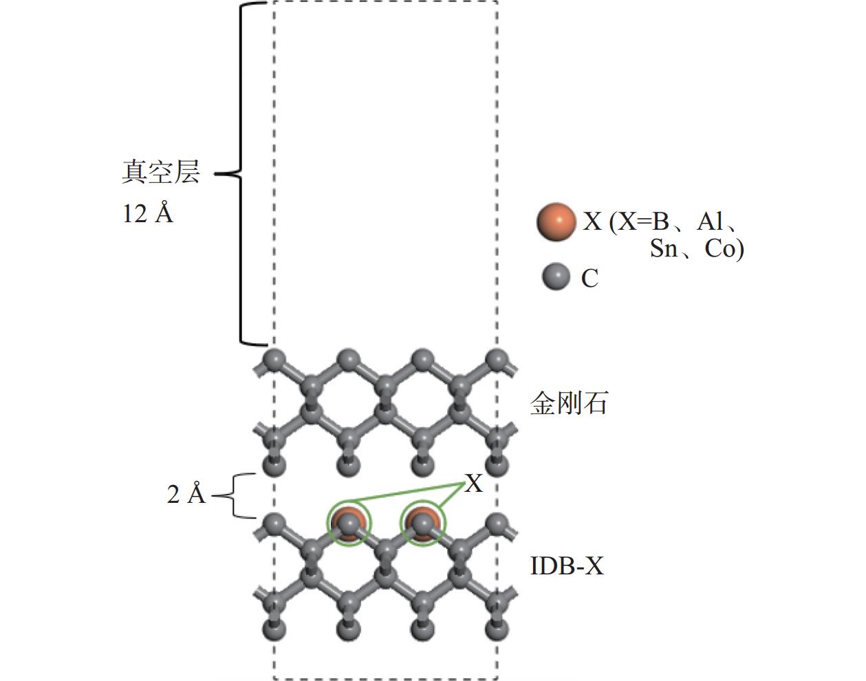
图 2 IDB-X/Diamond膜基界面模型图
Figure 2. IDB-X/Diamond membrane-based interface model diagram
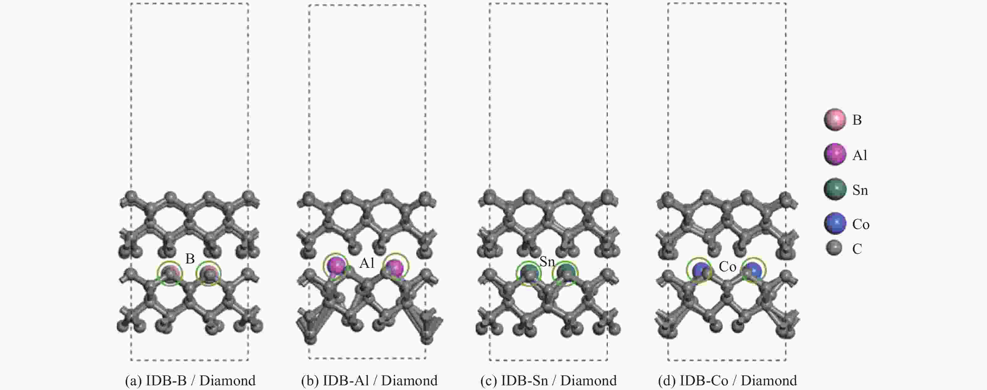
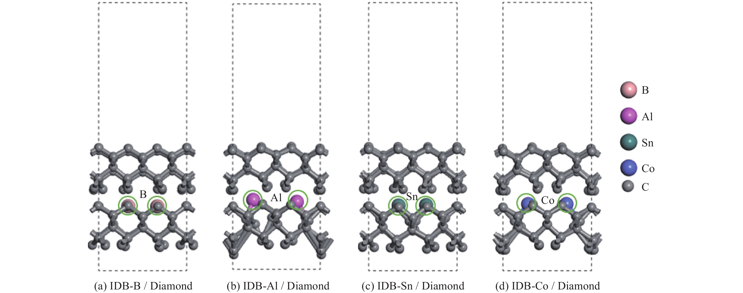
图 3 结构优化后的IDB-X/Diamond膜基界面模型
Figure 3. Optimized structure of IDB-X/Diamond membrane-based interface model

图 5 IDB-X/Diamond膜基界面差分电荷分布图
Figure 5. Differential charge distribution at IDB-X/Diamond membrane-based interface
表 1 IDB-X/Diamond膜基界面结合能
Table 1. IDB-X/Diamond membrane-based interface binding energy
掺杂元素 X EIDB-X / eV EDiamond / eV EIDB-X/Diamond / eV A / Å Wad-X /(J·m−2) B − 6773.67 − 6913.28 − 13728.42 56.90 11.68 Al − 6738.01 − 13686.58 9.94 Co − 8709.79 − 15649.28 7.38 Sn − 6812.62 − 13750.23 6.85  下载: 导出CSV
表 2 原子布居数
Table 2. Mulliken atomic population
掺杂元素X 原子种类 原子布居数 失电荷数 φ 有效电荷利用率 λ / % s p d 总电子数 n B C1 1.13 3.08 0.00 4.21 −0.21e 98 B 0.70 1.71 0.00 2.41 0.59e C2 1.16 3.02 0.00 4.18 −0.18e C3 1.16 3.03 0.00 4.19 −0.19e Al C1 1.21 3.22 0.00 4.43 −0.43e 58 Al 0.57 0.54 0.00 1.11 1.89e C2 1.17 3.19 0.00 4.36 −0.36e C3 1.16 3.15 0.00 4.31 −0.31e Sn C1 1.16 3.18 0.00 4.34 −0.34e 43 Sn 0.48 1.46 0.00 1.94 2.06e C2 1.16 3.11 0.00 4.27 −0.27e C3 1.15 3.13 0.00 4.28 −0.28e Co C1 1.23 3.00 0.00 4.23 −0.23e 39 Co 0.10 −0.60 7.79 7.29 1.71e C2 1.19 3.03 0.00 4.22 −0.22e C3 1.16 3.05 0.00 4.21 −0.21e 注:有效电荷利用率 = [−(φC1 + φC2 + φC3) / φX] ×100%,X = B、Al、Sn、Co。
下载: 导出CSV
表 3 化学键重叠布居数
Table 3. Overlapping population of chemical bonds
掺杂元素X 键 重叠布居数 键长 / Å B C1—B 1.07 1.490 C2—B 0.87 1.550 C3—B 0.87 1.540 Al C1—Al 0.60 1.822 C2—Al 0.57 1.858 C3—Al 0.03 1.955 Sn C1—Sn 0.53 1.923 C2—Sn 0.38 1.995 C3—Sn 0.36 1.989 Co C1—Co 0.26 1.882 C2—Co −0.17 1.886 C3—Co 0.24 1.907
下载: 导出CSV
-
[1] WANG H G, HUANG H C, BI W X, et al. Deep and ultra-deep oil and gas well drilling technologies: Progress and prospect [J]. Natural Gas Industry B,2022,9(2):141-157. doi: 10.1016/j.ngib.2021.08.019 [2] 李梦. 无硬质相胎体仿生异型齿孕镶金刚石钻头研究 [D]. 长春: 吉林大学, 2017.LI Meng. Research on no-hardphase-matrix impregnated diamond bit with bionic abnormal shape [D]. Changchun: Jilin University, 2017. [3] HSIEH Y Z, LIN S T. Diamond tool bits with iron alloys as the binding matrices [J]. Materials Chemistry and Physics,2001,72(2):121-125. doi: 10.1016/S0254-0584(01)00419-9 [4] 高雅. Ni、Sn对Fe基金刚石工具胎体组织及性能影响[D]. 北京: 机械科学研究总院, 2018.GAO Ya. Influence of Nickel and Tin on the microstructure and performance of Fe-based matrixes for diamond tools [D]. Beijing: General Academy of Mechanical Sciences, 2018. [5] 王恒, 杨展, 杨洋. 高磷-硼铁基胎体性能研究及应用 [J]. 金刚石与磨料磨具工程,2011,31(2):31-34. doi: 10.3969/j.issn.1006-852X.2011.02.007WANG Heng, YANG Zhan, YANG Yang. Study on the performance of high phosphor-boron-iron based matrix and their application [J]. Diamond & Abrasives Engineering,2011,31(2):31-34. doi: 10.3969/j.issn.1006-852X.2011.02.007 [6] FAN Y M, GUO H, XU J, et al. Effects of boron on the microstructure and thermal properties of Cu/diamond composites prepared by pressure infiltration [J]. International Journal of Minerals, Metallurgy, and Materials,2011,18(4):472-478. doi: 10.1007/s12613-011-0465-2 [7] 徐小健. 纳米材料改善孕镶金刚石钻头胎体性能研究 [D]. 长春: 吉林大学, 2015.XU Xiaojian. The properties study of nano material to improve the impregnated diamond bit matrix [D]. Changchun: Jilin University, 2015. [8] LI L, WEI Q P, MA L, et al. Preparation of cemented carbide diamond films by gaseous boronizing pretreatment combines with self-assembly seeding process [J]. International Journal of Refractory Metals and Hard Materials,2020,87:105173. doi: 10.1016/j.ijrmhm.2019.105173 [9] JOHNSTON J M, BAKER P, CATLEDGE S A. Improved nanostructured diamond adhesion on cemented tungsten carbide with boride interlayers [J]. Diamond and Related Materials,2016,69:114-120. doi: 10.1016/j.diamond.2016.08.006 [10] YE F, LI Y S, SUN X Y, et al. CVD diamond coating on WC-Co substrate with Al-based interlayer [J]. Surface and Coatings Technology,2016,308:121-127. doi: 10.1016/j.surfcoat.2016.06.088 [11] PARK J K, LEE H J, LEE W S, et al. Effect of TiAl-based interlayer on the surface morphology and adhesion of nanocrystalline diamond film deposited on WC–Co substrate by hot filament CVD [J]. Surface and Coatings Technology,2014,258:108-113. doi: 10.1016/j.surfcoat.2014.09.053 [12] LAI W C, WU Y S, CHANG H C, et al. Enhancing the adhesion of diamond films on cobalt-cemented tungsten carbide substrate using tungsten particles via MPCVD system [J]. Journal of Alloys and Compounds,2011,509(12):4433-4438. doi: 10.1016/j.jallcom.2011.01.149 [13] 简小刚, 何嘉诚, 王俊鹏, 等. 金属元素Co、Fe、Cu、Ti对孕镶金刚石基底CVD金刚石涂层膜基界面结合强度的影响 [J]. 真空科学与技术报,2019,39(1):58-64. doi: 10.13922/j.cnki.cjovst.2019.01.09JIAN Xiaogang, HE Jiacheng, WANG Junpeng, et al. Effect of metal dopant on interface adhesion of diamond coating on impregnated diamond substrate: A first principle calculation [J]. Chinese Journal of Vacuum Science and Technology,2019,39(1):58-64. doi: 10.13922/j.cnki.cjovst.2019.01.09 [14] HU J B, JIAN X G. Mechanism of Co atom point defects on different termination surfaces of WC–Co/diamond interface by first-principles [J]. Modern Physics Letters B,2022,36(19):2250074. doi: 10.1142/S0217984922500749 [15] 王杨. 硅衬底/铱/外延金刚石的第一性原理计算及实验研究 [D]. 哈尔滨: 哈尔滨工业大学, 2021.WANG Yang. First-principles calculation and experimental investigation of siliconsubstrate/iridium/epitaxialdiamond [D]. Harbin: Harbin Institute of Technology, 2021. [16] YANG J, HUANG J H, FAN D Y, et al. First-principles investigation on the electronic property and bonding configuration of NbC (111)/NbN (111) interface [J]. Journal of Alloys and Compounds,2016,689:874-884. doi: 10.1016/j.jallcom.2016.08.040 [17] SEGALL M D, SHAH R, PICKARD C J, et al. Population analysis of plane-wave electronic structure calculations of bulk materials [J]. Physical Review B,1996,54(23):16317. doi: 10.1103/PhysRevB.54.16317 [18] VIDAKIS N, ANTONIADIS A, BILALIS N. The VDI 3198 indentation test evaluation of a reliable qualitative control for layered compounds [J]. Journal of Materials Processing Technology,2003,143:481-485. doi: 10.1016/S0924-0136(03)00300-5 [19] SMITH E J W, PIRACHA A H, FIELD D, et al. Mixed-size diamond seeding for low-thermal-barrier growth of CVD diamond onto GaN and AlN [J]. Carbon,2020,167:620-626. doi: 10.1016/j.carbon.2020.05.050 -

 下载:
下载:


 点击查看大图
计量
- 文章访问数: 626
- HTML全文浏览量: 348
- PDF下载量: 17
- 被引次数: 0
 邮件订阅
邮件订阅 RSS
RSS