Numerical simulation and experiment of uniform growth of MPCVD diamond coating
-
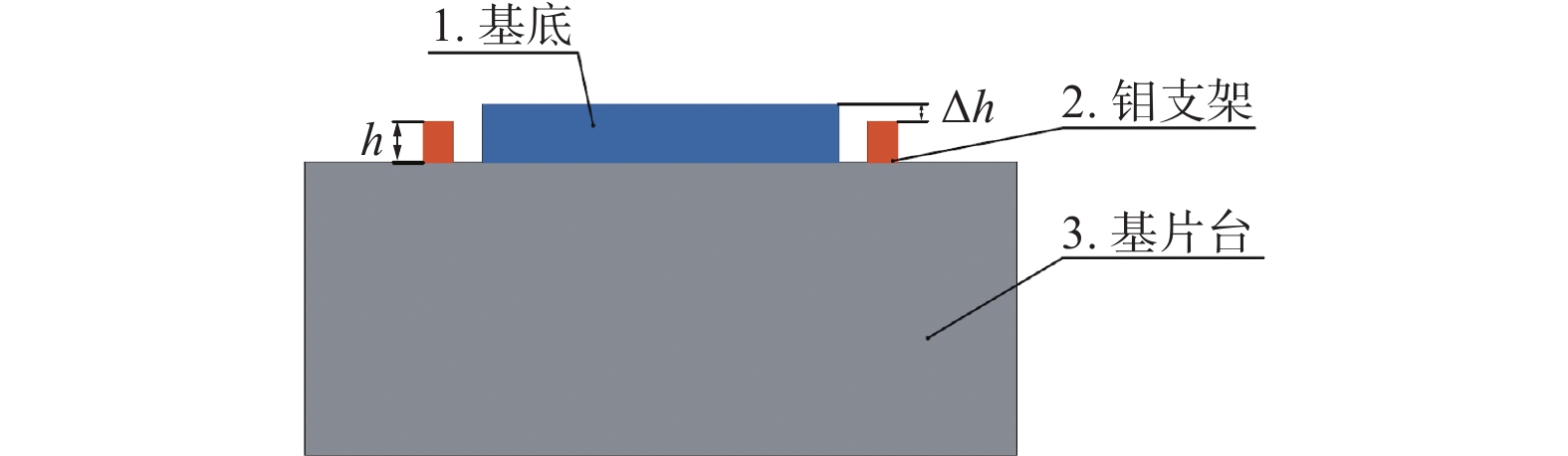
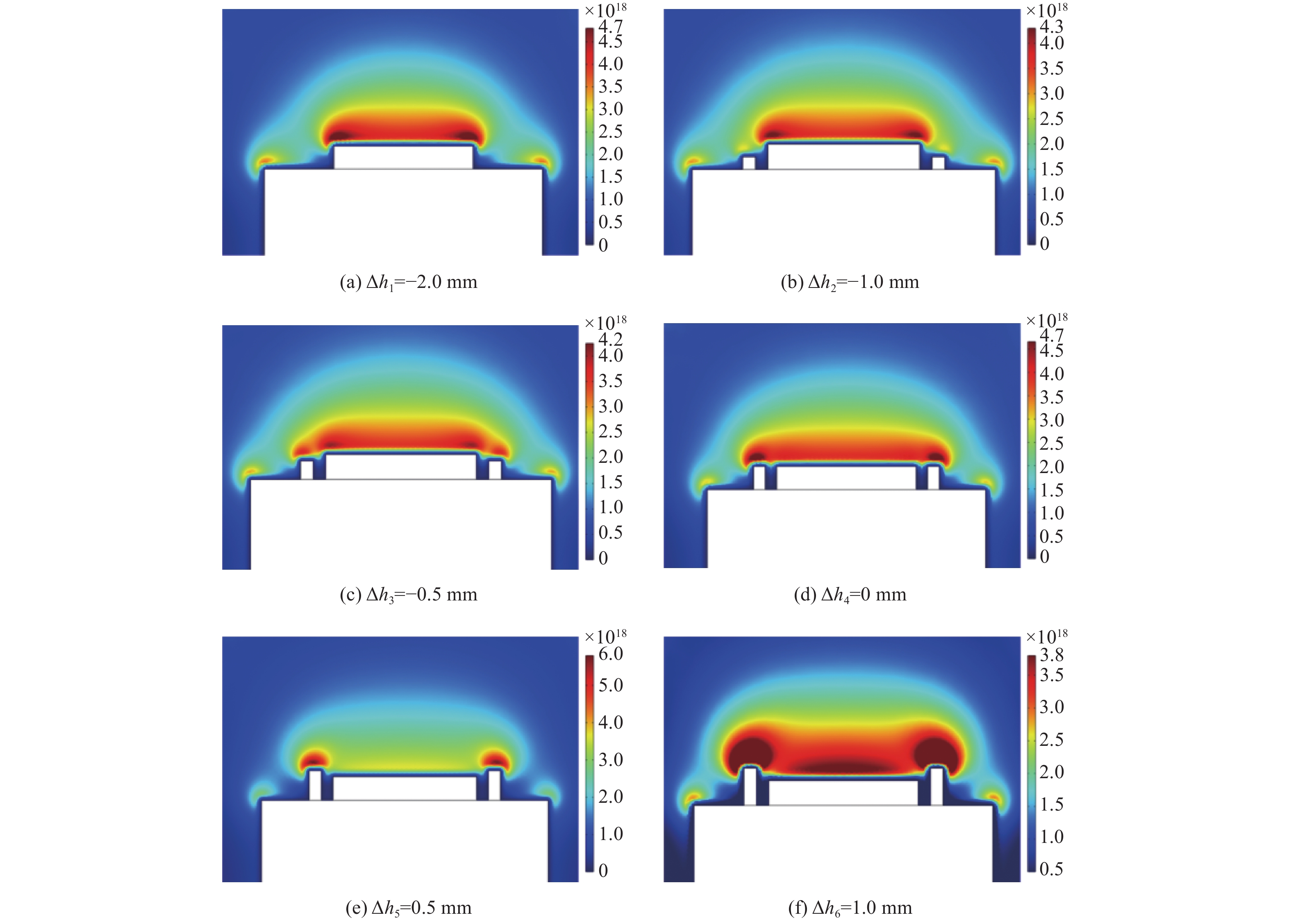
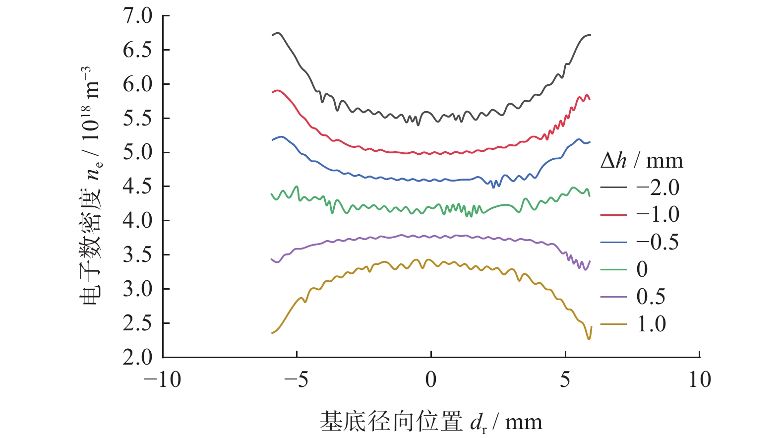
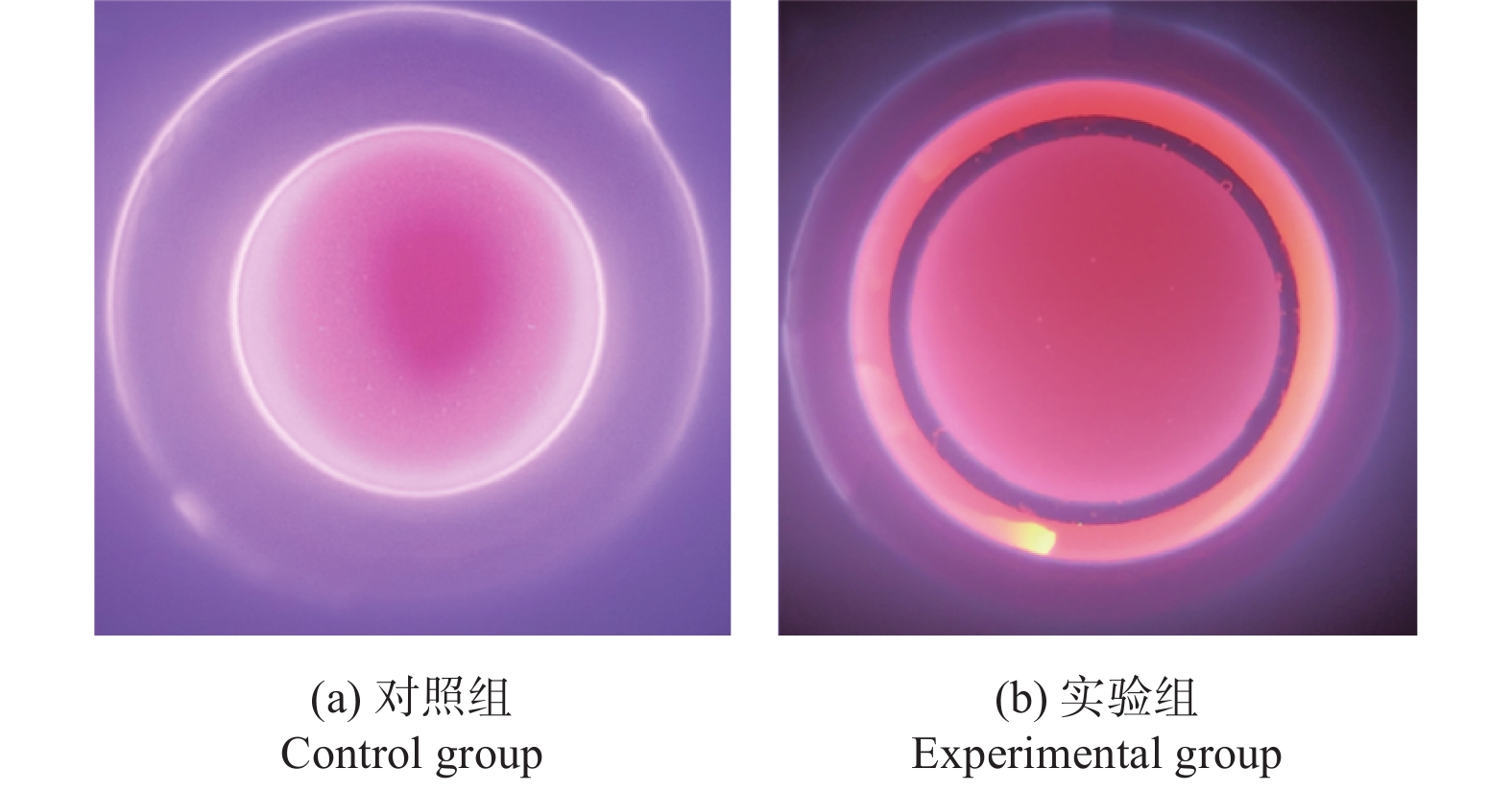
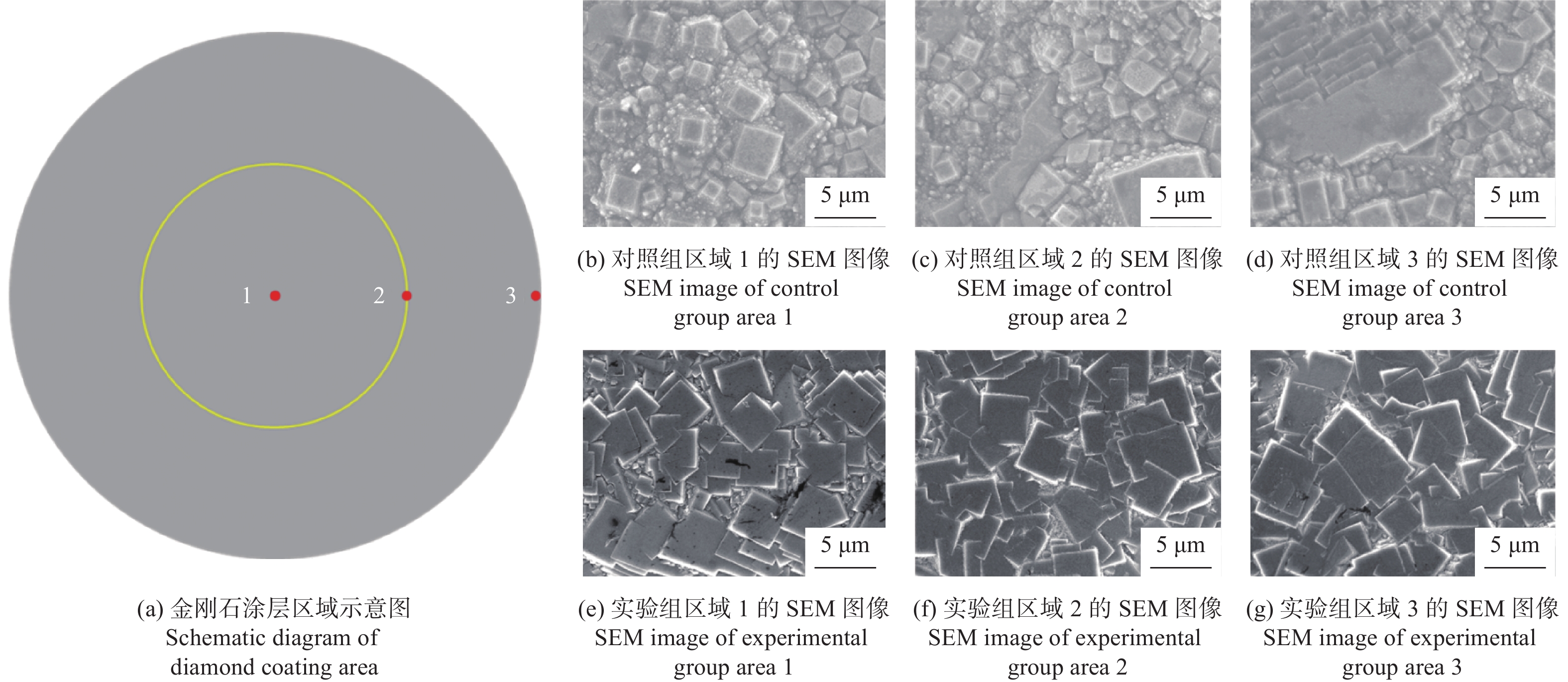
摘要: 基于多物理场耦合仿真软件COMSOL Multiphysics的微波等离子体模块建立MPCVD反应腔内氢气等离子体的仿真模型,研究基底外侧增设的环状钼支架与基底的不同高度差Δh对基底表面等离子体分布的影响。采用变异系数对等离子体分布的均匀性进行定量分析,并用SEM对金刚石涂层表面的微观形貌进行表征。结果表明:当Δh=0 mm时,等离子体分布的均匀性最佳,变异系数为3.998%,金刚石涂层的晶粒分布及大小的均匀性相较于无钼支架时的明显提升;当Δh<0 mm时,等离子体分布的均匀性随Δh增大而提升,变异系数由10.265%降至3.998%;当Δh>0 mm时,等离子体分布的均匀性不增反降,变异系数升高至10.048%。此外,当Δh=−2.0 mm时,基底表面的等离子体密度约下降20%,不利于金刚石涂层生长。Abstract: Based on the microwave plasma module of multiphysics simulation software COMSOL Multiphysics, a numerical model of hydrogen plasma inside a MPCVD reactor was built. The effect of different height differences Δh between the circular molybdenum support added on the outer side of the substrate and the substrate on the plasma distribution at the surface of the substrate was investigated. The uniformity of plasma distribution was quantitatively analyzed by coefficient of variation, and the microstructure of diamond coating surface was characterized by SEM. The results show that when Δh=0 mm, the uniformity of plasma distribution is the best, the coefficient of variation is 3.998%, and the uniformity of grain distribution and size of diamond coating is significantly improved compared with that without molybdenum support. When Δh< 0 mm, the uniformity of plasma distribution increases with the increase of Δh, and the coefficient of variation decreases from 10.265% to 3.998%. When Δh>0 mm, the uniformity of plasma distribution does not increased but decreases, and the coefficient of variation increases to 10.048%. In addition, when Δh=−2.0 mm, the plasma density on the substrate surface decreases by about 20%, which is not conducive to the growth of diamond coating.
-
Key words:
- diamond coating /
- uniformity /
- microwave plasma /
- numerical simulation
-
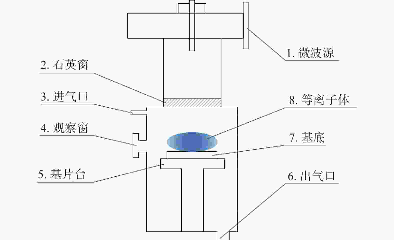
图 1 圆柱形金属谐振腔式MPCVD装置示意图
Figure 1. Schematic diagram of cylindrical metal resonant cavity MPCVD device
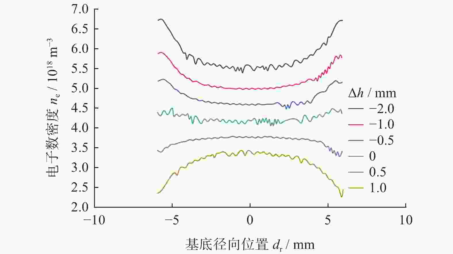
图 4 基底径向电子数密度分布图
Figure 4. Radial number density distribution of electrons on the substrate surface
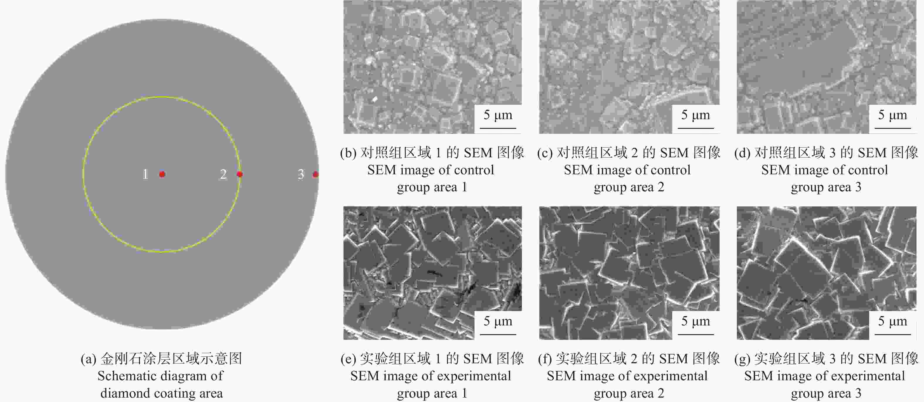
图 7 对照组和实验组的金刚石涂层不同区域的SEM图像
Figure 7. SEM images of different areas of diamond coating in control group and experimental group
表 1 原始数据及电子数密度的变异系数
Table 1. Original data and coefficients of variation of electron number density
高度差 Δh / mm 标准差 $\sigma $/ m−3 平均值 $\mu $/ m−3 变异系数 ${C_{\rm{v}}}$/% −2.0 3.918 × 10¹⁷ 3.817 × 10¹⁸ 10.265 −1.0 2.842 × 10¹⁷ 3.801 × 10¹⁸ 7.477 −0.5 2.233 × 10¹⁷ 3.649 × 10¹⁸ 6.119 0 1.516 × 10¹⁷ 3.792 × 10¹⁸ 3.998 0.5 1.504 × 10¹⁷ 3.497 × 10¹⁸ 4.301 1.0 3.131 × 10¹⁷ 3.116 × 10¹⁸ 10.048  下载: 导出CSV
表 2 实验工艺参数
Table 2. Process parameters
参数 形核 生长 基底温度 θ / ℃ 625 800 CH4流量 l1 / sccm 5.0 4.3 CO2流量 l2 / sccm 6.0 0 Ar流量 l3 / sccm 15 0 H2流量 l4 / sccm 200 200 压力 p / kPa 8 8 时间 t / h 2 7
下载: 导出CSV
表 3 沉积前后基底厚度
Table 3. Substrate thickness before and after deposition
测量区域 实验前厚度
d1 / mm沉积后厚度
d2 / mm厚度差
Δd / μm对照组基底中心 2.001 2.033 32 对照组基底边缘 2.006 2.044 38 实验组基底中心 1.997 2.021 24 实验组基底边缘 2.002 2.028 26
下载: 导出CSV
-
[1] LI G, RAHIM M Z, PAN W, et al. The manufacturing and the application of polycrystalline diamond tools: A comprehensive review [J]. Journal of Manufacturing Processes,2020,56(5):400-416. [2] BOLSHAKOV A P, RALCHENKO V G, YUROV V Y, et al. Enhanced deposition rate of polycrystalline CVD diamond at high microwave power densities [J]. Diamond & Related Materials,2019(97):107466. [3] CHENG H Y, YANG C Y, YANG L C, et al. Effective thermal and mechanical properties of polycrystalline diamond films [J]. Journal of Applied Physics,2018,123(16):165105. doi: 10.1063/1.5016919 [4] DAR M A, KIM Y S, ANSARI S G, et al. Comparative study of diamond films grown on silicon substrate using microwave plasma chemical vapor deposition and hot-filament chemical vapor deposition technique [J]. Korean Journal of Chemical Engineering,2006,22(5):770-773. [5] NAD S, GU Y, ASMUSSEN J. Growth strategies for large and high quality single crystal diamond substrates [J]. Diamond & Related Materials,2015(60):26-34. [6] WANG B, WENG J, WANG Z T, et al. Investigation on the influence of the gas flow mode around substrate on the deposition of diamond films in an overmoded MPCVD reactor chamber [J]. Vacuum,2020,182(1):109659. [7] 简小刚, 雷强, 张奎林. 热丝CVD金刚石涂层温度场补偿优化研究 [J]. 金刚石与磨料磨具工程,2016,36(6):15-19, 24.JIAN Xiaogang, LEI Qiang, ZHANG Kuilin. Optimization of HFCVD diamond coating deposition temperature compensating [J]. Diamond & Abrasives Engineering,2016,36(6):15-19, 24. [8] LI L, ZHAO C, ZHANG S, et al. Simulation of diamond synthesis by microwave plasma chemical vapor deposition with multiple substrates in a substrate holder [J]. Journal of Crystal Growth,2022(579):126457. doi: 10.1016/j.jcrysgro.2021.126457 [9] ASHKIHAZI E E, SEDOV V S, SOVYK D N, et al. Plateholder design for deposition of uniform diamond coatings on WC-Co substrates by microwave plasma CVD for efficient turning application [J]. Diamond & Related Materials,2017(75):169-175. [10] 王凤英, 孟宪明, 唐伟忠, 等. 圆柱谐振腔式MPCVD装置中氢、氩微波等离子体分布规律的数值模拟 [J]. 真空与低温,2008(3):157-163. doi: 10.3969/j.issn.1006-7086.2008.03.007WANG Fengying, MENG Xianming, TANG Weizhong, et al. Simulation of hydrogen and argon microwave plasmas in a cylindrical microwave plasma chemical vapor deposition reactor [J]. Vacuum & Cryogenics,2008(3):157-163. doi: 10.3969/j.issn.1006-7086.2008.03.007 [11] 安康, 刘小萍, 李晓静, 等. 新型高功率MPCVD金刚石膜装置的数值模拟与实验研究 [J]. 人工晶体学报,2015,44(6):1544-1550. doi: 10.3969/j.issn.1000-985X.2015.06.022AN Kang, LIU Xiaoping, LI Xiaojing, et al. Numerical simulation and experimental study of a novel high-power microwave plasma CVD reactor for diamond films deposition [J]. Journal of Synthetic Crystals,2015,44(6):1544-1550. doi: 10.3969/j.issn.1000-985X.2015.06.022 [12] HASSOUNI K, SILVA F, GICQUEL A. Modelling of diamond deposition microwave cavity generated plasmas [J]. Journal of Physics D:Applied Physics,2010,43(15):153001. doi: 10.1088/0022-3727/43/15/153001 [13] DERKAOUI N, ROND C, GRIES T, et al. Determining electron temperature and electron density in moderate pressure H2/CH4 microwave plasma [J]. Journal of Physics D:Applied Physics,2014,47(20):205201. doi: 10.1088/0022-3727/47/20/205201 [14] MESBAHI A, SILVA F, FARHAT S, et al. Hydrodynamics effects in high power density microwave plasma diamond growth reactors [J]. Journal of Physics:D Applied Physics,2013,46(38):385502-385516. doi: 10.1088/0022-3727/46/38/385502 [15] YAMADA H, CHAYAHARA A, MOKUNO Y. Simplified description of microwave plasma discharge for chemical vapor deposition of diamond [J]. Journal of Applied Physics,2007,101(6):063302. doi: 10.1063/1.2711811 [16] KEATCH R. Principles of plasma discharges and material processing[M]. New York: Microelectronics Journal, 1996: 804. [17] FÜNER M, WILD C, KOIDL P. Simulation and development of optimized microwave plasma reactors for diamond deposition [J]. Surface and Coatings Technology,1999(116/117/118/119):853-862. [18] PLEULER E, WILD C, FÜNER M, et al. The CAP-reactor, a novel microwave CVD system for diamond deposition [J]. Diamond and Related Materials,2002,11(3):467-471. [19] VIEHLAND L A, MASON E A. Transport properties of gaseous ions over a wide energy range 4 [J]. Atomic Data and Nuclear Data Tables,1995,60(1):37-95. doi: 10.1006/adnd.1995.1004 [20] SCOTT C D, FARHAT S, GICQUEL A, et al. Determining electron temperature and density in a hydrogen microwave plasma [J]. Journal of Thermophysics and Heat Transfer,1996,10(3):426-435. doi: 10.2514/3.807 [21] PLANO L S, SURENDRA M, GRAVES D B. Self-consistent dc glow-discharge simulations applied to diamond film deposition reactors [J]. Journal of Applied Physics,1992,71(10):5189-5198. doi: 10.1063/1.350575 [22] 邹帅, 唐中华, 吉亮亮, 等. 悬浮型微波共振探针在电负性容性耦合等离子体中电子密度的测量 [J]. 物理学报,2012,61(7):075204. doi: 10.7498/aps.61.075204ZOU Shuai, TANG Zhonghua, JI Liangliang, et al. Application of floating microwave resonator probe to the measurement of electron density in electronegative capacitively coupled plasma [J]. Acta Physica Sinica,2012,61(7):075204. doi: 10.7498/aps.61.075204 -


 点击查看大图

计量
- 文章访问数: 507
- HTML全文浏览量: 215
- PDF下载量: 98
- 被引次数: 0
 邮件订阅
邮件订阅 RSS
RSS