Research on the rapid growth and structure of ultra-nanocrystalline diamond thin films
-
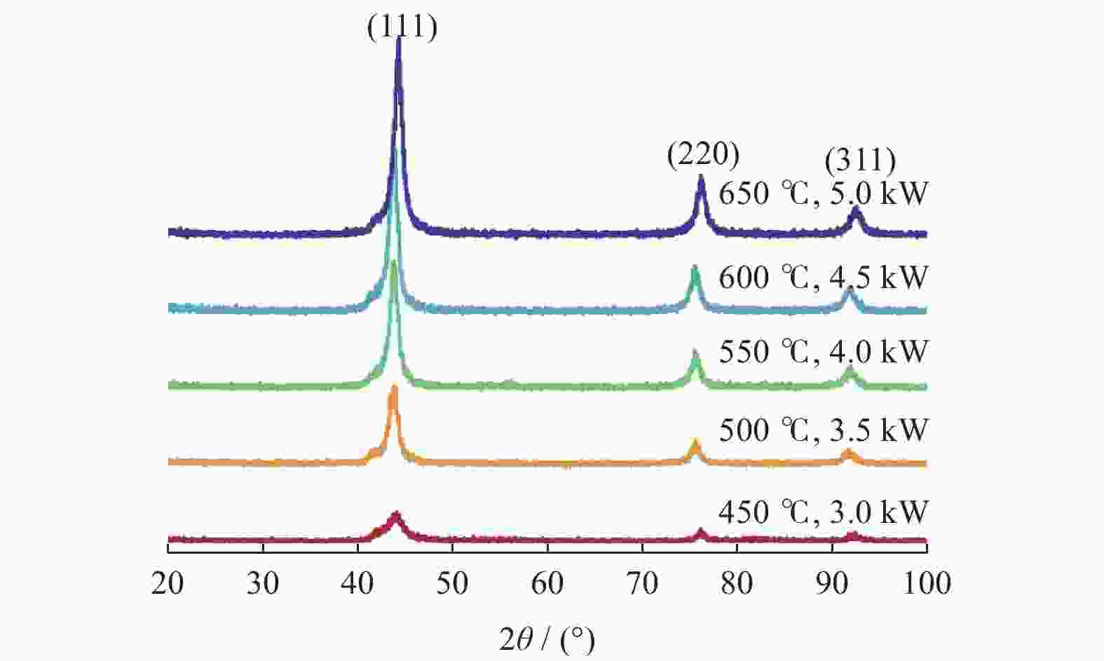
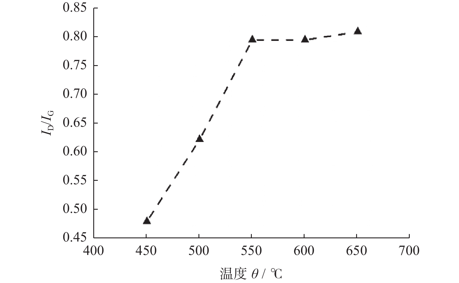
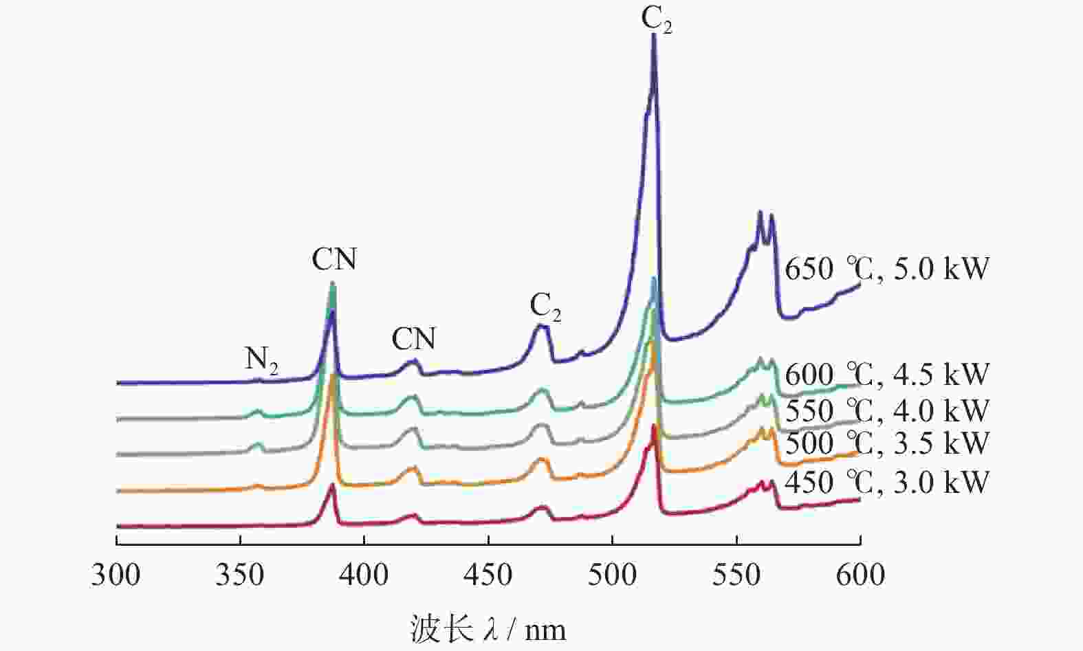
摘要: 采用微波等离子体化学气相沉积(microwave plasma chemical vapor deposition,MPCVD)技术,通过调节微波功率制备不同温度条件下的超纳米金刚石(ultrananocrystalline diamond,UNCD)薄膜。比较分析反应源激活功率及基体温度对UNCD膜生长和组成结构的影响,以期获得高质量UNCD膜材的快速生长工艺技术。采用SEM、XRD、Raman等方法分析表征UNCD薄膜的形貌结构、物相组成和生长速率,同时通过OES光谱监测UNCD薄膜沉积过程中的生长基团状态。结果表明:UNCD薄膜沉积的基体温度范围在450~650 ℃,且随着功率和基体温度增加,OES光谱中CN、C2基团峰值强度增强,生长速率从0.82 μm/h上升到6.62 μm/h;膜材中晶粒尺寸稍有增加,但平均晶粒尺寸均小于10.00 nm,且表面更加平整光滑,形成更有利于力学性能的表面形貌。因此,采用二异丙胺液态小分子为反应源,同时施加更高的微波功率,在更高的基体温度下沉积是快速生长高质量UNCD膜的有效工艺途径。Abstract: Ultra-nanocrystalline diamond (UNCD) films were prepared by microwave plasma chemical vapour deposition (MPCVD) at different temperature conditions by adjusting the microwave power. The effects of the activation power of the reaction source and effects of the temperature of the substrate on the growth and composition of the UNCD films were compared and analysed in order to obtain the technique to rapidly grow high-quality UNCD films. SEM, XRD and Raman methods were used to characterise the morphological structure, phase composition and growth rate of the UNCD films, while OES spectroscopy was used to monitor the state of the growth groups during the deposition of the UNCD films. The results showed that the deposition temperature of the UNCD films ranged from 450 to 650 ℃; that the peak intensity of CN and C2 groups in the OES spectra increased with the increase of power and substrate temperature; that the growth rate increased from 0.82 μm/h to 6.62 μm/h; and that the grain size in the films increased. The average grain size was less than 10.00 nm, and the surface was flatter and smoother, forming a surface profile more favourable to the mechanical properties. Therefore, the use of diisopropylamine liquid small molecules as the reaction source, together with the application of higher microwave power and deposition at higher substrate temperatures, is an effective way to mushroom high-quality UNCD films.
-
Key words:
- UNCD film /
- MPCVD /
- substrate temperature /
- growth rate; grain size
-
表 1 UNCD薄膜制备工艺参数
Table 1. Preparation process parameters of UNCD films
参数名称 数值 功率 P / kW 3.0 3.5 4.0 4.5 5.0 温度 θ / ℃ 450 500 550 600 650 压力 p / kPa 11.3 11.3 11.3 11.3 11.3 C6H15N流量 Q1 / (mL·min−1) 8 8 8 8 8 H2流量 Q2 / (mL·min−1) 160 160 160 160 160 表 2 不同微波功率及温度下沉积薄膜的厚度及生长速度
Table 2. Thickness and growth rate of deposited films under different microwave power and temperature
参数名称 数值 功率 P / kW 3.0 3.5 4.0 4.5 5.0 温度 θ / ℃ 450 500 550 600 650 3 h沉积厚度 h / μm 2.417 7.349 13.310 14.460 19.870 生长速率 v / (μm·h−1) 0.81 2.45 4.44 4.82 6.62 表 3 不同温度下UNCD薄膜的晶粒尺寸
Table 3. Grain size of UNCD films at different temperatures
功率
p/kW温度
θ / ℃衍射峰位
2θ / (°)半峰宽
B / (cm−1)由不同衍射峰
所得晶粒尺寸
d / nm平均晶粒尺寸
d1 / nm3.0 450 44.05 2.15 4.14 8.83 75.98 0.82 12.75 92.02 1.24 9.59 3.5 500 43.86 1.20 7.42 8.73 75.42 1.09 9.56 91.49 1.29 9.20 4.0 550 43.92 1.05 8.46 9.20 75.43 1.05 9.98 91.58 1.29 9.17 4.5 600 43.88 0.95 9.32 9.34 75.38 1.10 9.45 91.52 1.28 9.24 5.0 650 44.38 1.01 8.86 8.98 76.02 1.12 9.35 92.19 1.37 8.72 -
[1] AUCIELLO O, SUMANT A V. Status review of the science and technology of ultrananocrystalline diamond (UNCD™) films and application to multifunctional devices [J]. Diamond and Related Materials,2010,19(7/8/9):699-718. [2] AUCIELLO O. Science and technology of multifunctional ultrananocrystalline diamond (UNCDTM) coatings and applications to a new generation of implantable medical devices [J]. Journal of Biotechnology & Biomaterials,2017,7(2):6-7. [3] ZHOU A F, WANG X, PACHECO E, et al. Ultrananocrystalline diamond nanowires: Fabrication, characterization, and sensor applications [J]. Materials (Basel),2021,14(3):661. doi: 10.3390/ma14030661 [4] AUCIELLO O, ASLAM D M. Review on advances in microcrystalline, nanocrystalline and ultrananocrystalline diamond films-based micro/nano-electromechanical systems technologies [J]. Journal of Materials Science,2021,56(12):1-60. [5] SANKARAN K J, KURIAN J, CHEN H C, et al. Origin of a needle-like granular structure for ultrananocrystalline diamond films grown in a N2/CH4 plasma [J]. Journal of Physics D: Applied Physics, 2012, 45(36): 365303. [6] 谈耀麟. 论UNCD的应用与研发方向(工业金刚石战略发展思考之三) [J]. 超硬材料工程,2011,23(1):36-41. doi: 10.3969/j.issn.1673-1433.2011.01.009TAN Yaolin. On the application and R&D direction of UNCD (third thought on the strategic development of industrial diamond) [J]. Superabrasives Engineering,2011,23(1):36-41. doi: 10.3969/j.issn.1673-1433.2011.01.009 [7] SARAVANAN A, HUANG B R, SANKARAN K J, et al. Fast growth of ultrananocrystalline diamond films by bias-enhanced nucleation and growth process in CH4/Ar plasma [J]. Applied Physics Letters,2014,104(18):1603-1605. [8] TANG C J, NEVES A J, PEREIRA S, et al. Effect of nitrogen and oxygen addition on morphology and texture of diamond films (from polycrystalline to nanocrystalline) [J]. Diamond and Related Materials,2008,17(1):72-78. doi: 10.1016/j.diamond.2007.10.022 [9] LIN Q, CHEN S, JI Z, et al. A novel growth model for depositing ultrananocrystalline diamond films in CH4/H2 chemistry [J]. Surface and Coatings Technology,2021,419(12):72-80. [10] SANKARAN K J, HUANG B-R, SARAVANAN A, et al. Nitrogen incorporated ultrananocrystalline diamond microstructures from bias-enhanced microwave N2/CH4-plasma chemical vapor deposition [J]. Plasma Processes and Polymers,2016,13(4):419-428. doi: 10.1002/ppap.201500079 [11] ARENAL R, BRUNO P, MILLER D J, et al. Diamond nanowires and the insulator-metal transition in ultrananocrystalline diamond films [J]. Physical Review B,2007,75(19):434-436. [12] BHATTACHARYYA S, AUCIELLO O, BIRRELL J, et al. Synthesis and characterization of highly-conducting nitrogen-doped ultrananocrystalline diamond films [J]. Applied Physics Letters,2001,79(10):1441-1443. doi: 10.1063/1.1400761 [13] 马志斌, 吴建鹏, 陶利平, 等. MPCVD等离子体的发射光谱研究 [J]. 光谱学与光谱分析,2013,33(9):2562-2565. doi: 10.3964/j.issn.1000-0593(2013)09-2562-04MA Zhibin, WU Jianpeng, TAO Liping, et al. Emission spectroscopic study of MPCVD plasma [J]. Spectroscopy and Spectral Analysis,2013,33(9):2562-2565. doi: 10.3964/j.issn.1000-0593(2013)09-2562-04 [14] 陶利平. MPCVD沉积金刚石薄膜光谱分析 [D]. 武汉: 武汉工程大学, 2013.TAO Liping. Spectral analysis of MPCVD deposited diamond film [D]. Wuhan: Wuhan Institute of Technology, 2013. [15] 叶嗣林, 王天乐, 黄国波, 等. MPCVD法制备的不同温度的金刚石涂层的微结构及力学性能研究 [J]. 广州化工,2021,49(23):31-34. doi: 10.3969/j.issn.1001-9677.2021.23.010YE Silin, WANG Tianle, HUANG Guobo, et al. Study on microstructure and mechanical properties of diamond coatings prepared by MPCVD method at different temperatures [J]. Guangzhou Chemical Industry,2021,49(23):31-34. doi: 10.3969/j.issn.1001-9677.2021.23.010 [16] 江彩义, 髙冀芸, 郭胜惠, 等. 氧气流量对MPCVD法制备超纳米金刚石膜的影响 [J]. 材料导报,2017,31(S1):66-69.JIANG Caiyi, GAO Jiyun, GUO Shenghui, et al. Effect of oxygen flow rate on the preparation of ultra-nanodiamond films by MPCVD [J]. Materials Direct,2017,31(S1):66-69. [17] PANDA K, KUMAR N, PANIGRAHI B K, et al. Tribological properties of N+ ion implanted ultrananocrystalline diamond films [J]. Tribology International,2013,57:124-136. doi: 10.1016/j.triboint.2012.07.016 [18] SANKARAN K J, KUMAR N, KURIAN J, et al. Improvement in tribological properties by modification of grain boundary and microstructure of ultrananocrystalline diamond films [J]. Acs Appl Mater Interfaces,2013,5(9):3614-3624. doi: 10.1021/am303144m -


 下载:
下载:


 邮件订阅
邮件订阅 RSS
RSS
